
Datasheet


TEMT6200FX01
www.vishay.com
Vishay Semiconductors
Rev. 1.9, 25-Jun-14
2
Document Number: 81317
For technical questions, contact: detectortechsupport@vishay.com
THIS DOCUMENT IS SUBJECT TO CHANGE WITHOUT NOTICE. THE PRODUCTS DESCRIBED HEREIN AND THIS DOCUMENT
ARE SUBJECT TO SPECIFIC DISCLAIMERS, SET FORTH AT www.vishay.com/doc?91000
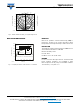
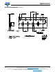
Fig. 1 - Power Dissipation Limit vs. Ambient Temperature
Note
• Each 3000 piece packing unit will contain a single group. The label on the bag will indicate which binned group is in the bag. A specific group
cannot be ordered. Production shipments containing multiple bags will likely include multiple groups. Please design accordingly.
020406080
0
25
50
75
100
125
P
V
- Power Dissipation (mW)
T
amb
- Ambient Temperature (°C)
100
94 8308
R
thJA
= 450 K/W
BASIC CHARACTERISTICS (T
amb
= 25 °C, unless otherwise specified)
PARAMETER TEST CONDITION SYMBOL MIN. TYP. MAX. UNIT
Collector emitter breakdown voltage I
C
= 0.1 mA V
CEO
6V
Collector dark current V
CE
= 5 V, E = 0 lx I
CEO
350nA
Collector emitter capacitance V
CE
= 0 V, f = 1 MHz, E = 0 lx C
CEO
16 pF
Photo current
E
V
= 20 lx, CIE illuminant A, V
CE
= 5 V I
PCE
4.6 μA
E
V
= 100 lx, CIE illuminant A, V
CE
= 5 V I
PCE
7.5 23 39 μA
Temperature coefficient of I
PCE
CIE illuminant A TK
IPCE
1.18 %/K
LED, white TK
IPCE
0.9 %/K
Angle of half sensitivity ϕ ± 60 deg
Wavelength of peak sensitivity λ
p
550 nm
Range of spectral bandwidth λ
0.5
450 to 610 nm
Collector emitter saturation voltage E
V
= 20 lx, 0.45 μA V
CEsat
0.1 V
TYPE DEDICATED CHARACTERISTICS (T
amb
= 25 °C, unless otherwise specified)
PARAMETER TEST CONDITION
BINNED
GROUP
SYMBOL MIN. MAX. UNIT
Photo current
E
V
= 100 lx,
CIE illuminant A,
V
CE
tz51 = 5 V
AI
PCE
7.5 15 μA
BI
PCE
12 24 μA
CI
PCE
19.5 39 μA