
Datasheet


TSOP22.., TSOP24.., TSOP48.., TSOP44..
www.vishay.com
Vishay Semiconductors
Rev. 1.3, 05-Feb-14
2
Document Number: 82459
THIS DOCUMENT IS SUBJECT TO CHANGE WITHOUT NOTICE. THE PRODUCTS DESCRIBED HEREIN AND THIS DOCUMENT
ARE SUBJECT TO SPECIFIC DISCLAIMERS, SET FORTH AT www.vishay.com/doc?91000
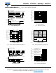
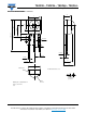
BLOCK DIAGRAM APPLICATION CIRCUIT
Note
• Stresses beyond those listed under “Absolute Maximum Ratings” may cause permanent damage to the device. This is a stress rating only
and functional operation of the device at these or any other conditions beyond those indicated in the operational sections of this specification
is not implied. Exposure to absolute maximum rating condtions for extended periods may affect the device reliability.
33 kΩ
2
3
1
Demo-
pass
AGCInput
PIN
Band
dulator
Control circuit
16833_14
C
1
IR receiver
GND
Circuit
µC
R
1
+ V
S
GND
Transmitter
with
TSALxxxx
V
S
V
O
17170-10
OUT
The external components R
1
and C
1
are optional
to improve the robustness against electrical overstress
(typical values are R
1
= 100 Ω, C
1
= 0.1 µF).
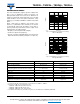
ABSOLUTE MAXIMUM RATINGS
PARAMETER TEST CONDITION SYMBOL VALUE UNIT
Supply voltage V
S
-0.3 to +6 V
Supply current I
S
5mA
Output voltage V
O
-0.3 to 5.5 V
Voltage at output to supply V
S
- V
O
-0.3 to (V
S
+ 0.3) V
Output current I
O
5mA
Junction temperature T
j
100 °C
Storage temperature range T
stg
-25 to +85 °C
Operating temperature range T
amb
-25 to +85 °C
Power consumption T
amb
≤ 85 °C P
tot
10 mW
Soldering temperature t ≤ 10 s, 1 mm from case T
sd
260 °C
ELECTRICAL AND OPTICAL CHARACTERISTICS (T
amb
= 25 °C, unless otherwise specified)
PARAMETER TEST CONDITION SYMBOL MIN. TYP. MAX. UNIT
Supply current
E
v
= 0, V
S
= 5 V I
SD
0.55 0.7 0.9 mA
E
v
= 40 klx, sunlight I
SH
0.8 mA
Supply voltage V
S
2.5 5.5 V
Transmission distance
E
v
= 0, test signal see fig. 1,
IR diode TSAL6200,
I
F
= 200 mA
d45m
Output voltage low
I
OSL
= 0.5 mA, E
e
= 0.7 mW/m
2
,
test signal see fig. 1
V
OSL
100 mV
Minimum irradiance
Pulse width tolerance:
t
pi
- 5/f
o
< t
po
< t
pi
+ 6/f
o
,
test signal see fig. 1
E
e min.
0.12 0.25 mW/m
2
Maximum irradiance
t
pi
- 5/f
o
< t
po
< t
pi
+ 6/f
o
,
test signal see fig. 1
E
e max.
50 W/m
2
Directivity
Angle of half transmission
distance
ϕ
1/2
± 45 deg