
Datasheet

VEMD2500X01, VEMD2520X01
www.vishay.com
Vishay Semiconductors
Rev. 1.2, 18-Oct-11
4
Document Number: 83294
For technical questions, contact: detectortechsupport@vishay.com
THIS DOCUMENT IS SUBJECT TO CHANGE WITHOUT NOTICE. THE PRODUCTS DESCRIBED HEREIN AND THIS DOCUMENT
ARE SUBJECT TO SPECIFIC DISCLAIMERS, SET FORTH AT www.vishay.com/doc?91000
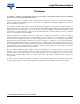
REFLOW SOLDER PROFILE
Fig. 7 - Lead (Pb)-free Reflow Solder Profile acc. J-STD-020D
DRYPACK
Devices are packed in moisture barrier bags (MBB) to
prevent the products from moisture absorption during
transportation and storage. Each bag contains a desiccant.
FLOOR LIFE
Floor life (time between soldering and removing from MBB)
must not exceed the time indicated on MBB label:
Floor life: 4 weeks
Conditions: T
amb
< 30 °C, RH < 60 %
Moisture sensitivity level 2a, acc. to J-STD-020.
DRYING
In case of moisture absorption devices should be baked
before soldering. Conditions see J-STD-020 or label.
Devices taped on reel dry using recommended conditions
192 h at 40 °C (+ 5 °C), RH < 5 %.
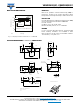
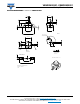
PACKAGE DIMENSIONS in millimeters: VEMD2500X01
0
50
100
150
200
250
300
0 50 100 150 200 250 300
Time (s)
Temperature (°C)
240 °C
245 °C
max. 260 °C
max. 120 s
max. 100 s
217 °C
max. 30 s
max. ramp up 3 °C/s
max. ramp down 6 °C/s
19841
255 °C
2.2
5.8 ± 0.2
2.77 ± 0.2
2.3 ± 0.2
Cathode
0.5
0.05 ± 0.1
0.254
1.1 ± 0.1
Anode
0.4
2.2
0.19
0.3
1.6
0.4
Z
Ø 1.8 ± 0.1
2.3 ± 0.2
specications
according to DIN
technical drawings
Not indicated tolerances ± 0.1
Drawing-No.: 6.544-5391.02-4
Pin ID
exposed copper
Issue: 2; 18.03.10
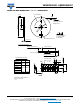
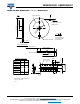
21517
0.75
6.7
1.7
Ø 2.3 ± 0.1
Solder pad proposal
acc. IPC 7351
Z 20:1