
Datasheet


VEMD5510C
www.vishay.com
Vishay Semiconductors
Rev. 1.0, 22-Jun-17
1
Document Number: 84354
For technical questions, contact: detectortechsupport@vishay.com
THIS DOCUMENT IS SUBJECT TO CHANGE WITHOUT NOTICE. THE PRODUCTS DESCRIBED HEREIN AND THIS DOCUMENT
ARE SUBJECT TO SPECIFIC DISCLAIMERS, SET FORTH AT www.vishay.com/doc?91000
Silicon PIN Photodiode
DESCRIPTION
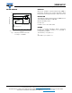
VEMD5510C is a high speed and high sensitive PIN
photodiode. It is a low profile surface-mount device (SMD)
including the chip with a 7.5 mm
2
sensitive area detecting
visible light much like the human eye. The diode has its
peak sensitivity at 550 nm and a low capacitance.
FEATURES
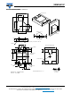
• Package type: surface-mount
• Package form: top view
• Dimensions (L x W x H in mm): 5 x 4 x 0.9
• Radiant sensitive area (in mm
2
): 7.5
• High photo sensitivity
• Suppression filter for near infrared radiation
• Fast response times
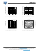
• Angle of half sensitivity: ϕ = ± 65°
• Floor life: 72 h, MSL 4, according to
J-STD-020
• Material categorization: for definitions of compliance
please see www.vishay.com/doc?99912
APPLICATIONS
• Wearables
• Optical heart rate monitoring
• Ambient light sensors
Note
• Test conditions see table “Basic Characteristics”
Note
• MOQ: minimum order quantity
PRODUCT SUMMARY
COMPONENT I
ra
(μA) ϕ (deg) λ
0.5
(nm)
VEMD5510C 0.6 ± 65 440 to 700
ORDERING INFORMATION
ORDERING CODE PACKAGING REMARKS PACKAGE FORM
VEMD5510C Tape and reel MOQ: 1000 pcs, 1000 pcs/reel Top view
VEMD5510C-GS15 Tape and reel MOQ: 5000 pcs, 5000 pcs/reel Top view
ABSOLUTE MAXIMUM RATINGS (T
amb
= 25 °C, unless otherwise specified)
PARAMETER TEST CONDITION SYMBOL VALUE UNIT
Reverse voltage V
R
20 V
Power dissipation T
amb
≤ 25 °C P
V
215 mW
Junction temperature T
j
110 °C
Operating temperature range T
amb
-40 to +100 °C
Storage temperature range T
stg
-40 to +100 °C
Soldering temperature According to reflow solder profile Fig. 8 T
sd
260 °C
Thermal resistance junction-to-ambient R
thJA
350 K/W
ESD safety HBM ± 2000 V, 1.5 kΩ, 100 pF, 3 pulses ESD
HBM
≥ 2 kV