
Datasheet


VEMD5510C
www.vishay.com
Vishay Semiconductors
Rev. 1.0, 22-Jun-17
4
Document Number: 84354
For technical questions, contact: detectortechsupport@vishay.com
THIS DOCUMENT IS SUBJECT TO CHANGE WITHOUT NOTICE. THE PRODUCTS DESCRIBED HEREIN AND THIS DOCUMENT
ARE SUBJECT TO SPECIFIC DISCLAIMERS, SET FORTH AT www.vishay.com/doc?91000
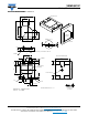
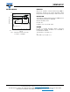
PACKAGE DIMENSIONS in millimeters
1
1
5.2
1
Center of device
Recommended footprint
4.1
Optical
window
Top view
Bottom view
Detail X ( 20 : 1 )
0.2
0.1
4
5
2.1
1.8
3
3
Optical
center
1.8
Detail X
0.9 ± 0.15
Tie bar, electrically connected to cathode
0.8
1.2
0.9
1.2
2.5
0.8
0.6 (4 x)
3.1
Exposed pad
(cathode)
0.4 (4 x)
2
2
Cathode
0.6
NC
Anode
0.65
0.8
Drawing- No.: 6.550-5329.01-4
Issue: 3; 11.11.2016
Not indicated tolerances ± 0.1
Technical drawings
according to DIN
specication