
Datasheet

VEMT2000X01, VEMT2020X01
www.vishay.com
Vishay Semiconductors
Rev. 1.3, 23-Aug-11
2
Document Number: 81595
For technical questions, contact: detectortechsupport@vishay.com
THIS DOCUMENT IS SUBJECT TO CHANGE WITHOUT NOTICE. THE PRODUCTS DESCRIBED HEREIN AND THIS DOCUMENT
ARE SUBJECT TO SPECIFIC DISCLAIMERS, SET FORTH AT www.vishay.com/doc?91000
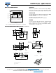
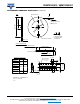
Fig. 1 - Power Dissipation Limit vs. Ambient Temperature
Power power dissipation T
amb
75 °C P
V
100 mW
Junction temperature T
j
100 °C
Operating temperature range T
amb
- 40 to + 100 °C
Storage temperature range T
stg
- 40 to + 100 °C
Soldering temperature Acc. reflow profile fig. 8 T
sd
260 °C
Thermal resistance junction/ambient Acc. J-STD-051 R
thJA
250 K/W
ABSOLUTE MAXIMUM RATINGS (T
amb
= 25 °C, unless otherwise specified)
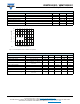
PARAMETER TEST CONDITION SYMBOL VALUE UNIT
0
20
40
60
80
100
120
0 102030405060708090100
21619
R
thJA
= 250 K/W
T
amb
- Ambient Temperature (°C)
P
V
- Power Dissipation (mW)
BASIC CHARACTERISTICS (T
amb
= 25 °C, unless otherwise specified)
PARAMETER TEST CONDITION SYMBOL MIN. TYP. MAX. UNIT
Collector emitter breakdown voltage I
C
= 0.1 mA V
CEO
20 V
Collector dark current V
CE
= 5 V, E = 0 I
CEO
1 100 nA
Collector emitter capacitance V
CE
= 0 V, f = 1 MHz, E = 0 C
CEO
25 pF
Collector light current
E
e
= 1 mW/cm
2
, = 950 nm,
V
CE
= 5 V
I
ca
369mA
Angle of half sensitivity ± 15 deg
Wavelength of peak sensitivity
p
860 nm
Range of spectral bandwidth
0.5
790 to 970 nm
Collector emitter saturation voltage I
C
= 0.05 mA V
CEsat
0.4 V
Temperature coefficient of I
ca
E
e
= 1 mW/cm
2
, = 950 nm,
V
CE
= 5 V
Tk
Ica
1.1 %/K