
Datasheet

VOT8121AM
www.vishay.com
Vishay Semiconductors
Rev. 1.2, 30-Oct-2018
2
Document Number: 84914
For technical questions, contact: optocoupleranswers@vishay.com
THIS DOCUMENT IS SUBJECT TO CHANGE WITHOUT NOTICE. THE PRODUCTS DESCRIBED HEREIN AND THIS DOCUMENT
ARE SUBJECT TO SPECIFIC DISCLAIMERS, SET FORTH AT www.vishay.com/doc?91000
Note
• Stresses in excess of the absolute maximum ratings can cause permanent damage to the device. Functional operation of the device is not
implied at these or any other conditions in excess of those given in the operational sections of this document. Exposure to absolute
maximum ratings for extended periods of the time can adversely affect reliability.
This phototriac should not be used to drive a load directly. It is intended to be a trigger device only
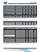
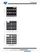
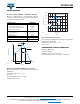
Fig. 1 - Maximum Forward Current vs. Ambient Temperature Fig. 2 - Maximum On-State Current vs. Ambient Temperature
ABSOLUTE MAXIMUM RATINGS (T
amb
= 25 °C, unless otherwise specified)
PARAMETER TEST CONDITION SYMBOL VALUE UNIT
INPUT
Reverse voltage V
R
6V
Forward current I
F
50 mA
Power dissipation P
diss
70 mW
OUTPUT
Peak off-state voltage V
DRM
800 V
RMS on-state current I
T(RMS)
100 mA
Power dissipation P
diss
300 mW
Peak repetitive surge current PW = 1 ms, 120 pps I
TSM
1A
COUPLER
Storage temperature range T
stg
-55 to +150 °C
Ambient temperature range T
amb
-55 to +110 °C
Total power dissipation P
diss
330 mW
Soldering temperature For 10 s T
sld
260 °C
10
100
1000
10000
0
10
20
30
40
50
60
-60 -40 -20 0 20 40 60 80 100 120
Axis Title
1st line
2nd line
2nd line
I
F max.
- Maximum Forward Current (mA)
T
amb
- Ambient Temperature (°C)
10
100
1000
10000
0
20
40
60
80
100
120
-60 -40 -20 0 20 40 60 80 100 120
Axis Title
1st line
2nd line
2nd line
I
T max.
- Maximum On-State Current (A
RMS
)
T
amb
- Ambient Temperature (°C)