WT8266-S2WiFiModule Extreme / Open / Small / Easy Specification Version 2.
Disclaimer and Copyright Notice Information in this document, including URL references, is subject to change without notice. THIS DOCUMENT IS PROVIDED AS IS WITH NO WARRANTIES WHATSOEVER, INCLUDING ANYWARRANTY OF MERCHANTABILITY, NON‐INFRINGEMENT, FITNESS FOR ANY PARTICULARPURPOSE, OR ANY WARRANTY OTHERWISE ARISING OUT OF ANY PROPOSAL, SPECIFICATIONOR SAMPLE. All liability, including liability for infringement of any proprietary rights, relating to useof information in this document is disclaimed.
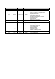
Version V1.0 Changed by Lemme Time Reason 2015.08.13 Original Details Flash size Available RAM size Power consumption on deep sleep mode Operating Temperature Model size on top view Schematic of WT8266-S2 FCC/CE/RoHs certification document Tech support email Product picture Environment temperature V2.0 Lemme 2015.10.12 Update V2.1 Lemme 2015.10.18 Update V2.2 Lemme 2015.12.29 Update CE Caution V2.3 Lemme 2016.1.21 Update CE marking update V2.4 Lemme 2016.1.
Contents 1.Overview.................................................................................................................................................... 5 2. Main Features ........................................................................................................................................... 5 3. Hardware Specifications ........................................................................................................................... 6 3.1 System Diagram ...........
1. Overview WT8266‐S2 Wi‐Fi module is a low consumption, high performance Wi‐Fi network control module designed by Wireless‐Tag. It can meet the IoT application requirements in smart power grids, building automation, security and protection, smart home, remote health care etc.
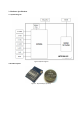
3. Hardware Specifications 3.1 System Diagram WT8266‐S2 Figure‐1System Diagram 3.
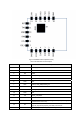
Figure‐3 WT8266‐S2 Pinout (Bottom View) Table 1 Pin Definition and Description Pin Name Description 1 VDD 3.3V supply(VDD) 2 IO4 GPIO4 3 IO0 GPIO0 4 IO2 GPIO2;UART1_TXD 5 IO15 GPIO15;MIDO; HSPICS;UART0_RTS 6 GND GND 7 IO13 GPIO13; HSPI_MOSI;UART0_CTS 8 IO5 GPIO5 9 RX0 UART0_RXD;GPIO3 10 GND GND 11 TX0 UART0_TXD;GPIO1 12 RST Reset Module 13 ADC 14 EN 15 IO16 Detecting chip VDD3P3 supply voltage or ADC pin input voltage (not available at the same time) Chip Enable.
16 IO12 GPIO12;HSPI_MISO 17 IO14 GPIO14;HSPI_CLK 18 GND GND 19 GND GND PAD Note: Table‐2 Pin Mode Mode IO15 IO0 IO2 UART Download Mode Low Low High Flash Boot Mode Low High High Table‐3 Interface Description Name Pin HSPI Interface IO12(MISO),IO13(MOSI),I O14(CLK),IO15(CS) PWM Interface IO12(R),IO15(G),IO13(B) IR Interface ADC Interface I2C Interface UART Interface IO14(IR_T), IO5(IR_R) ADC IO14(SCL), IO2(SDA) UART0: TX0(U0TXD),RX0(U0RXD), IO15(RTS),IO13(CTS) UART1: IO2(TX
3.3Electrical Characteristic 3.3.1Maximum Ratings Table‐ 4. Maximum Ratings Ratings Condition Value Unit Storage Temperature / ‐45 to 125 °C Maximum Soldering Temperature / 260 °C Supply Voltage IPC/JEDEC J‐STD‐020 +3.0 to +3.6 V 3.3.2Recommended Operating Environment Table ‐5 Recommended Operating Environment Working Environment Operating Temperature Name Min Value Typical Values Max Value Unit / ‐40 20 85 °C VDD 3.0 3.3 3.6 V Supply Voltage 3.3.
3.4.2Standby Power Consumption Thefollowingcurrentconsumptionisbasedon3.3Vsupplyand25°Cambientwith internalregulators.ValuesaremeasuredatantennaportwithoutSAWfilter.Allthe transmissionmeasurementsvaluesarebasedon90%dutycycle,continuoustransmission mode. Table ‐8 Standby Power Consumption Mode Status Typical Value Modem Sleep 15mA Light Sleep 0.9mA Deep Sleep 20uA Off 0.5uA Standby Power Save Mode (2.4G) (Low Power Listen disabled) ¹ DTIM period Current Cons.
3.5.2 RF Tx Characteristics Table‐10 Emission Characteristics Mark Parameters Condition Min Value Typical Value Max Value Unit Ftx Input Frequency — 2.412 — 2.484 GHz Output Power Pout 11b 1Mbps — 19.5 — dBm 11Mbps — 18.5 — dBm 54Mbps — 16 — dBm MCS7 — 14 — dBm 3.5.3RF Rx Characteristics Table‐11RF Receiving Characteristics Mark Parameters Condition Min Value Typical Value Max Value Unit Frx Input Frequency — 2.412 — 2.
Figure ‐4 Module Size (Front View)
Figure ‐4‐1 Module Size (reverse projection view) Figure ‐5 Module Size (Side View) 3.
4.2 Schematics Figure ‐7 WT8266‐S2 Schematics 5.
6. Product Trial Forum:bbs.wireless-tag.
Federal Communication Commission Statement (FCC, U.S.) This equipment has been tested and found to comply with the limits for a Class B digital device, pursuant to Part 15 of the FCC Rules. These limits are designed to provide reasonable protection against harmful interference in a residential installation. This equipment generates, uses and can radiate radio frequency energy and, if not installed and used in accordance with the instructions, may cause harmful interference to radio communications.
combination with the host equipment is no longer considered valid and the FCC ID of the module cannot be used on the final product. In these circumstances, the OEM integrator will be responsible for re‐evaluating the end product (including the transmitter) and obtaining a separate FCC authorization. End product labeling: The final end product must be labeled in a visible area with the following: “Contains Transmitter Module FCC ID: 2AFOS‐WT8266‐S2”.
Information that must be placed in the end user manual: The OEM integrator has to be aware not to provide information to the end user regarding how to install or remove this RF module in the user's manual of the end product which integrates this module. The end user manual shall include all required regulatory information/warning as show in this manual.
Integration instructions for host product manufacturers according to KDB 996369 D03 OEM Manual v01 2.2 List of applicable FCC rules FCC Part 15 Subpart C 15.247 & 15.207 & 15.209 2.3 Specific operational use conditions The module is a WIFI module with WIFI 2.4G function. Operation Frequency: 2412~2462MHz Number of Channel: 11 Modulation: 802.11b CCK; 802.11g/n OFDM Type: FPC Antenna Gain: 3 dBi Max. The module can be used for mobile or applications with a maximum 3dBi antenna.
Host product manufacturers need to provide a physical or e‐label stating “Contains FCC ID: 2AFOS‐ WT8266‐S2”with their finished product.
2.9 Information on test modes and additional testing requirements Operation Frequency: 2412~2462MHz Number of Channel: 11 Modulation: 802.11b CCK; 802.11g/n OFDM Host manufacturer must perfom test of radiated & conducted emission and spurious emission, etc according to the actual test modes for a stand‐alone modular transmitter in a host, as well as for multiple simultaneously transmitting modules or other transmitters in a host product.
FCC STATEMENT : This device complies with Part 15 of the FCC Rules. Operation is subject to the following two conditions: (1) This device may not cause harmful interference, and (2) This device must accept any interference received, including interference that may cause undesired operation. Warning: Changes or modifications not expressly approved by the party responsible for compliance could void the user's authority to operate the equipment.