
Specifications

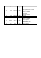
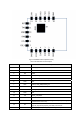


Figure‐3WT8266‐S2Pinout(BottomView)
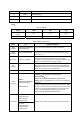
Table1PinDefinitionandDescription
Pin Name Description
1 VDD
3.3Vsupply(VDD)
2 IO4 GPIO4
3 IO0 GPIO0
4 IO2 GPIO2;UART1_TXD
5 IO15 GPIO15;MIDO;HSPICS;UART0_RTS
6 GND GND
7 IO13 GPIO13;HSPI_MOSI;UART0_CTS
8 IO5 GPIO5
9 RX0 UART0_RXD;GPIO3
10 GND GND
11 TX0 UART0_TXD;GPIO1
12 RST ResetModule
13 ADC
DetectingchipVDD3P3supplyvoltageorADCpininputvoltage(not
availableatthesametime)
14 EN
ChipEnable.
High:On,chipworksproperly;Low:Off,smallcurrent
15 IO16 GPIO16;Deepsleepwakeup,byconnectingtoRSTpin