
Datasheet
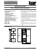

X9C102/103/104/503
2
PIN DESCRIPTIONS
V
H
and V
L
The high (V
H
) and low (V
L
) terminals of the X9C102/103/
104/503 are equivalent to the fixed terminals of a
mechanical potentiometer. The minimum voltage is –5V
and the maximum is +5V. It should be noted that the
terminology of V
L
and V
H
references the relative position
of the terminal in relation to wiper movement direction
selected by the U/D input and not the voltage potential on
the terminal.
V
W
V
W
is the wiper terminal, equivalent to the movable
terminal of a mechanical potentiometer. The position
of the wiper within the array is determined by the
control inputs. The wiper terminal series resistance is
typically 40Ω.
Up/Down (U/
DD
DD
D)
The U/D input controls the direction of the wiper
movement and whether the counter is incremented or
decremented.
Increment (
INCINC
INCINC
INC)
The INC input is negative-edge triggered. Toggling INC
will move the wiper and either increment or decrement
the counter in the direction indicated by the logic level on
the U/D input.
Chip Select (
CSCS
CSCS
CS)
The device is selected when the CS input is LOW. The
current counter value is stored in nonvolatile memory
when CS is returned HIGH while the INC input is also
HIGH. After the store operation is complete the X9C102/
103/104/503 will be placed in the low power standby
mode until the device is selected once again.
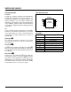
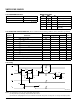
PIN CONFIGURATION
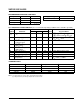
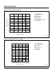
PIN NAMES
Symbol Description
V
H
High Terminal
V
W
Wiper Terminal
V
L
Low Terminal
V
SS
Ground
V
CC
Supply Voltage
U/D Up/Down Input
INC Increment Input
CS Chip Select Input
NC No Connect
3863 PGM T01
V
CC
CS
V
L
V
W
3863 FHD F02.2
INC
U/D
V
H
V
SS
1
2
3
4
8
7
6
5
X9C102/
103/104/503
DIP/SOIC