
Datasheet

X9C102/103/104/503
4
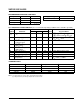
ABSOLUTE MAXIMUM RATINGS*
Temperature under Bias .................. –65°C to +135°C
Storage Temperature ....................... –65°C to +150°C
Voltage on CS, INC, U/D and V
CC
with Respect to V
SS
...............................
–1V to +7V
Voltage on V
H
and V
L
Referenced to V
SS
.................................
–8V to +8V
∆V = |V
H
–V
L
|
X9C102............................................................. 4V
X9C103, X9C503, and X9C104...................... 10V
Lead Temperature (Soldering, 10 seconds).... +300°C
Wiper Current ..................................................... ±1mA
*COMMENT
Stresses above those listed under “Absolute Maximum
Ratings” may cause permanent damage to the device.
This is a stress rating only and the functional operation
of the device at these or any other conditions above
those listed in the operational sections of this specifica-
tion is not implied. Exposure to absolute maximum
rating conditions for extended periods may affect device
reliability.
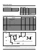
ANALOG CHARACTERISTICS
Electrical Characteristics
End-to-End Resistance Tolerance ..................... ±20%
Power Rating at 25°C
X9C102....................................................... 16mW
X9C103, X9C503, and X9C104.................. 10mW
Wiper Current ............................................ ±1mA Max.
Typical Wiper Resistance......................... 40Ω at 1mA
Typical Noise.......................... < –120dB/ Hz Ref: 1V
Resolution
Resistance ............................................................. 1%
Linearity
Absolute Linearity
(1)
........................................
±1.0 Ml
(2)
Relative Linearity
(3)
..................................... ±0.2 Ml
(2)
Temperature Coefficient
(–40°C to +85°C)
X9C102 ......................................+600 ppm/°C Typical
X9C103, X9C503, X9C104 ........+300 ppm/°C Typical
Ratiometric Temperature Coefficient ............ ±20 ppm
Wiper Adjustability
Unlimited Wiper Adjustment (Non-Store operation)
Wiper Position Store Operations ................... 10,000
Data Changes
Physical Characteristics
Marking Includes
Manufacturer‘s Trademark
Resistance Value or Code
Date Code
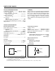
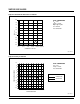
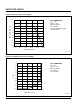
Test Circuit #1 Test Circuit #2
3863 FHD F04 3863 FHD F05
FORCE
CURRENT
V
L
V
W
V
H
TEST POINT
TEST POINT
V
W
V
H
V
L
Notes: (1) Absolute Linearity is utilized to determine actual wiper voltage versus expected voltage
= (V
w(n)
(actual) – V
w(n)
(expected)) = ±1 Ml Maximum.
(2) 1 Ml = Minimum Increment = R
TOT
/99.
(3) Relative Linearity is a measure of the error in step size between taps = V
W(n+1)
– [V
w(n)
+ Ml] = +0.2 Ml.