
North AmEricAN


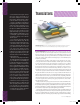

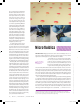


IllustratIon by Emily Cooper
Transistors
in a tech wo rld dominated by plastic, glass, and silicon, it may come as a
surprise to learn that research into paper electronics actually dates back nearly
50 years. In the late 1960s, Peter Brody’s group at Westinghouse Electric Corp.
experimented with paper, among other materials, as a substrate for thin-film tran-
sistors, the sort that could be built into switching arrays to control individual pixels
in a liquid-crystal display.
Even then, before a wealth of coating and processing innovations came on the
scene, paper had a number of attractive attributes. Chief among those was its quality
as an electrical insulator. Paper generally boasts a resistivity of some 10 billion
ohm-centimeters, about 100 000 times the intrinsic resistivity of silicon. That means
the material should, in theory, work quite well as a substrate for electronic devices.
Itresists the flow of current so well that it effectively eliminates one of the most com-
mon pathways electrons use to sneak across a transistor when it’s supposed to be off.
That isn’t to say paper is the ideal material on which to build transistors. Materials
like glass and traditional semiconductors are easy to manufacture with variations in
surface height of a few nanometers or less. But height variations in paper range from
at best a fraction of a micrometer up to several micrometers, depending on the fiber
size and how well those fibers commingle to form a flat mat. Electronic devices built
on such an irregular surface are likely to vary greatly in performance, and a sizable
proportion will not work at all.
Despite that, about five years ago, as interest in electronic readers and flexible reflec-
tive displays took off, researchers began to explore paper as an electronics substrate.
The potential payoff was big: If they could build the back-end circuitry needed to control
pixels, they’d be halfway to creating a changeable reflective display that naturally has
the look and feel of paper (and is just as thin, lightweight, and flexible).
Since then, about a half-dozen research groups have made considerable headway in
constructing paper-based transistors. They’ve used either inorganic semi conductors
like silicon or indium gallium zinc oxide for the current-carrying channels or organic
materials like pentacene or P3HT. A good part of this progress has followed from finding
flexIble stack: Transistors on flexible substrates can be built using organic or inorganic
semiconducting channels. This schematic illustrates a way of making an organic switch.
as new, bendable forms of glass. And at a
microscopic level it’s just a tangle of cel-
lulose bers, hardly the sort of structure
that’s ideal for making a bunch of nely
featured, identical circuit components.
But paper actually has a lot going for it.
It’s lightweight, exible, biodegradable,
and it comes from a renewable resource.
It’s also extraordinarily adaptable: With
the right set of additives and manufactur-
ing processes, paper can take on a seem-
ingly endless range of properties. It can be
made hydrophilic or hydrophobic, porous
or watertight, opaque or nearly transpar-
ent, delicate or strong, coarse or about as
smooth as glass.
Paper electronics also have the poten-
tial to be extraordinarily cheap. The ma-
terial itself is intrinsically inexpensive;
conventional varieties cost about a tenth
as much as plastic lm. Even the special
paper that’s tailor-made for electronics
costs, area for area, about 1 percent as
much as silicon. Roll-to-roll presses can
print microscopic features on wide reams
at speeds of up to 30 meters per second—
about three times as fast as the Olympian
Usain Bolt can run.
When my research group at the Univer-
sity of Cincinnati rst started working with
paper in 2008, we weren’t thinking too
broadly about the material’s potential as
the base layer, or substrate, for electronics.
We were originally interested in a relatively
narrow application, what might be called
“e-paper on paper,” essentially electronic
displays built directly on paper. The ini-
tial proof-of-principle experiment worked
far better than we expected, and in the
years since, I’ve become convinced that
paper’s potential could be just as broad
(ifnot as deep) as silicon’s has turned out
to be. Paper has already shown promise as
a substrate for sensors, biological assays,
RF antennas, batteries, circuit boards, and
smart packaging labels. In the next few
years, we’ll start to see the rst gadgets
based on this technoloy make their way
out of the laboratory and into the hands
of consumers and business users.
Channel
Drain
Source
Dielectric
Gate
Paper substrate
Previous Pages: adam Zocco/andrew J. steckl/university of cincinnati
02.PaperElectronics.NA.indd 50 1/17/13 1:16 PM