
Data Sheet


© 2009 Microchip Technology Inc. DS22088C-page 5
MCP3422/3/4
1.0 ELECTRICAL
CHARACTERISTICS
Absolute Maximum Ratings†
V
DD
...................................................................................7.0V
All inputs and outputs ............. ..........V
SS
–0.4V to V
DD
+0.4V
Differential Input Voltage ...................................... |V
DD
- V
SS
|
Output Short Circuit Current ................................Continuous
Current at Input Pins ....................................................±2 mA
Current at Output and Supply Pins ............................±10 mA
Storage Temperature ....................................-65°C to +150°C
Ambient Temp. with power applied ...............-55°C to +125°C
ESD protection on all pins ................ ≥ 6kV HBM, ≥ 400V MM
Maximum Junction Temperature (T
J
)..........................+150°C
†Notice: Stresses above those listed under “Maximum Rat-
ings” may cause permanent damage to the device. This is a
stress rating only and functional operation of the device at
those or any other conditions above those indicated in the
operational listings of this specification is not implied.
Exposure to maximum rating conditions for extended periods
may affect device reliability
.
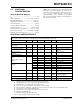
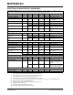
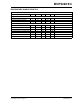
ELECTRICAL CHARACTERISTICS
Electrical Specifications: Unless otherwise specified, all parameters apply for T
A
= -40°C to +85°C, V
DD
= +5.0V, V
SS
= 0V,
CHn+ = CHn- = V
REF
/2, V
INCOM
= V
REF
/2. All ppm units use 2*V
REF
as differential full scale range.
Parameters Sym Min Typ Max Units Conditions
Analog Inputs
Differential Full Scale Input
Voltage Range
FSR — ±2.048/PGA — V V
IN
= [CHn+ - CHn-]
Maximum Input Voltage Range V
SS
-0.3 — V
DD
+0.3 V (Note 1)
Differential Input Impedance Z
IND
(f) — 2.25/PGA — MΩ During normal mode operation
(Note 2)
Common Mode input
Impedance
Z
INC
(f) — 25 — MΩ PGA = 1, 2, 4, 8
System Performance
Resolution and No Missing
Codes
(Effective Number of Bits)
(Note 3)
12 — — Bits DR = 240 SPS
14 — — Bits DR = 60 SPS
16 — — Bits DR = 15 SPS
18 — — Bits DR = 3.75 SPS
Data Rate
(Note 4)
DR 176 240 328 SPS 12 bits mode
44 60 82 SPS 14 bits mode
11 15 20.5 SPS 16 bits mode
2.75 3.75 5.1 SPS 18 bits mode
Output Noise — 1.5 — µV
RMS
T
A
= +25°C, DR = 3.75 SPS,
PGA = 1, V
IN
+ = V
IN
- = GND
Integral Non-Linearity INL — 10 35
ppm of
FSR
DR = 3.75 SPS, FSR = Full
Scale Range (Note 5)
Internal Reference Voltage V
REF
—2.048 — V
Gain Error (Note 6) — 0.05 0.35 % PGA = 1, DR = 3.75 SPS
Note 1: Any input voltage below or greater than this voltage causes leakage current through the ESD diodes at the input pins.
This parameter is ensured by characterization and not 100% tested.
2: This input impedance is due to 3.2 pF internal input sampling capacitor.
3: This parameter is ensured by design and not 100% tested.
4: The total conversion speed includes auto-calibration of offset and gain.
5: INL is the difference between the endpoints line and the measured code at the center of the quantization band.
6: Includes all errors from on-board PGA and V
REF
.
7: This parameter is ensured by characterization and not 100% tested.
8: MCP3423 and MCP3424 only.
9: Addr_Float voltage is applied at address pin.
10: No voltage is applied at address pin (left “floating”).