
Data Sheet


MCP3422/3/4
DS22088C-page 6 © 2009 Microchip Technology Inc.
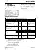
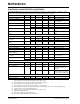
PGA Gain Error Match (Note 6) — 0.1 — % Between any 2 PGA settings
Gain Error Drift (Note 6) — 15 — ppm/°C PGA=1, DR=3.75 SPS
Offset Error V
OS
— 15 55 µV Tested at PGA = 1
DR = 3.75 SPS
Offset Drift vs. Temperature — 50 — nV/°C
Common-Mode Rejection — 105 — dB at DC and PGA =1,
— 110 — dB at DC and PGA =8, T
A
= +25°C
Gain vs. V
DD
— 5 — ppm/V T
A
= +25°C, V
DD
= 2.7V to 5.5V,
PGA = 1
Power Supply Rejection at DC
Input
— 100 — dB T
A
= +25°C, V
DD
= 2.7V to 5.5V,
PGA = 1
Power Requirements
Voltage Range V
DD
2.7 — 5.5 V
Supply Current during
Conversion
I
DDA
— 145 180 µA V
DD
= 5.0V
— 135 — µA V
DD
= 3.0V
Supply Current during Standby
Mode
I
DDS
—0.3 1µAV
DD
= 5.0V
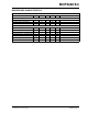
I
2
C Digital Inputs and Digital Outputs
High level input voltage V
IH
0.7V
DD
—V
DD
V at SDA and SCL pins
Low level input voltage V
IL
— — 0.3V
DD
V at SDA and SCL pins
Low level output voltage V
OL
—— 0.4VI
OL
= 3 mA
Hysteresis of Schmidt Trigger
for inputs (Note 7)
V
HYST
0.05V
DD
——Vf
SCL
= 100 kHz
Supply Current when I
2
C bus
line is active
I
DDB
— — 10 µA Device is in standby mode while
I
2
C bus is active
Input Leakage Current I
ILH
—— 1µAV
IH
= 5.5V
I
ILL
-1 — — µA V
IL
= GND
Logic Status of I
2
C Address Pins (Note 8)
Adr0 and Adr1 Pins Addr_Low V
SS
—0.2V
DD
V The device reads logic low.
Adr0 and Adr1 Pins Addr_High 0.75V
DD
—V
DD
V The device reads logic high.
Adr0 and Adr1 Pins Addr_Float 0.35V
DD
—0.6V
DD
V Read pin voltage if voltage is
applied to the address pin.
(Note 9)
—V
DD
/2 — Device outputs float output
voltage (V
DD
/2) on the address
pin, if left “floating”. (Note 10)
Pin Capacitance and I
2
C Bus Capacitance
Pin capacitance C
PIN
—4 10pF
I
2
C Bus Capacitance C
b
—— 400pF
ELECTRICAL CHARACTERISTICS (CONTINUED)
Electrical Specifications: Unless otherwise specified, all parameters apply for T
A
= -40°C to +85°C, V
DD
= +5.0V, V
SS
= 0V,
CHn+ = CHn- = V
REF
/2, V
INCOM
= V
REF
/2. All ppm units use 2*V
REF
as differential full scale range.
Parameters Sym Min Typ Max Units Conditions
Note 1: Any input voltage below or greater than this voltage causes leakage current through the ESD diodes at the input pins.
This parameter is ensured by characterization and not 100% tested.
2: This input impedance is due to 3.2 pF internal input sampling capacitor.
3: This parameter is ensured by design and not 100% tested.
4: The total conversion speed includes auto-calibration of offset and gain.
5: INL is the difference between the endpoints line and the measured code at the center of the quantization band.
6: Includes all errors from on-board PGA and V
REF
.
7: This parameter is ensured by characterization and not 100% tested.
8: MCP3423 and MCP3424 only.
9: Addr_Float voltage is applied at address pin.
10: No voltage is applied at address pin (left “floating”).