
Data Sheet


© 2009 Microchip Technology Inc. DS22088C-page 9
MCP3422/3/4
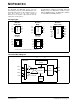
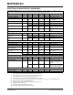
2.0 TYPICAL PERFORMANCE CURVES
Note: Unless otherwise indicated, T
A
= -40°C to +85°C, V
DD
= +5.0V, V
SS
= 0V, CHn+ = CHn- = V
REF
/2,
V
INCOM
= V
REF
/2.
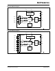
FIGURE 2-1: INL vs. Supply Voltage
(V
DD
).
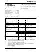
FIGURE 2-2: INL vs. Temperature.
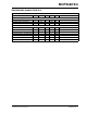
FIGURE 2-3: Offset Error vs.
Temperature.
FIGURE 2-4: Output Noise vs. Input
Voltage.
FIGURE 2-5: Total Error vs. Input Voltage.
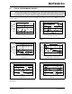
FIGURE 2-6: Gain Error vs. Temperature.
Note: The graphs and tables provided following this note are a statistical summary based on a limited number of
samples and are provided for informational purposes only. The performance characteristics listed herein
are not tested or guaranteed. In some graphs or tables, the data presented may be outside the specified
operating range (e.g., outside specified power supply range) and therefore outside the warranted range.
0
0.0005
0.001
0.0015
0.002
0.0025
0.003
0.0035
2.5 3 3.5 4 4.5 5 5.5
V
DD
(V)
Integral Non-Linearity
(% of FSR)
PGA = 8
PGA = 4
PGA = 1
PGA = 2
T
A
= +25°C
0
0.0005
0.001
0.0015
0.002
0.0025
0.003
0.0035
-60 -40 -20 0 20 40 60 80 100 120 140
Temperature (
o
C)
Integral Non-Linearity
(% of FSR)
2.7V
5V
5.5
V
PGA = 1
-20
-15
-10
-5
0
5
10
15
20
-60 -40 -20 0 20 40 60 80 100 120 140
Temperature (°C)
Offset Error (µV)
PGA = 1
PGA = 2
PGA = 4
PGA = 8
0
1
2
3
4
5
6
7
8
-100 -75 -50 -25 0 25 50 75 100
Input Signal (% of FSR)
OutPut Noise (µV,rms)
PGA = 1
PGA = 2
PGA = 4
PGA = 8
T
A
= +25°C
-2
-1.5
-1
-0.5
0
0.5
1
1.5
2
-100 -75 -50 -25 0 25 50 75 100
Input Voltage (% of Full-Scale)
Total Error (mV)
PGA = 1
PGA = 8
PGA = 4
PGA = 2
T
A
= +25°C
-0.6
-0.5
-0.4
-0.3
-0.2
-0.1
0
0.1
0.2
-60 -40 -20 0 20 40 60 80 100 120 140
Temperature (°C)
Gain Error (% of FSR)
PGA = 1
PGA = 2
PGA = 4
PGA = 8