
Specifications


Output Stage Biasing
www.ti.com
The LME49830 has a maximum DC bias voltage of 16V for use with just about any MOSFET device. The
high output drive current from the LME49830 makes it ideal for very high power amplifier applications.
5.1 V
BE
Multiplier
The LME49830’s BIAS
P
and BIAS
M
pins are available to create the DC bias of the output stage.
Depending on the device characteristics and design goals, a thermally compensated circuit may be
needed in order to have stable bias at the desired current across temperature. A non-compensated bias
circuit would consist of a resistor or potentiometer and one or two capacitors between the BIAS pins of the
LME49830. The EF125WT1 FET PCB uses a thermally compensated V
BE
multiplier for the bias circuit with
the Toshiba 2SK1530/2SJ201 devices in the output stage.
The V
BE
multiplier’s transistor, which needs to be mounted directly next to one of the power transistors on
the heat sink, will sense the output device's temperature with some temperature gradient through the
common heat sink. With a correctly designed V
BE
multiplier circuit the bias current of the output stage will
remain relatively stable over the device temperature operating range.
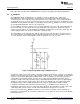
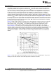
The V
BE
multiplier circuit created by Q
VBE1
with associated resistors and capacitors is shown in Figure 7.
The output stage bias can initially be adjusted through potentiometer, R
P1
in order to optimize for lowest
crossover distortion, desired sound quality or mode of operation – Class A, B, or AB.
Figure 7. Output Stage DC Biasing V
BE
Multiplier Circuit
The DC bias voltage can be measured by connecting a voltmeter between pins 1 and 2 of J
9
. The DC bias
voltage is measured from gate-to-gate of the output stage. When R
P1
is set at its minimum, the total output
stage bias current will be approximately 500mA. When set at its maximum, the total output stage bias
current will be approximately 175mA. The bias current setting of the EF125WT1 FET module before
leaving the factory, and for all performance data, is approximately 225mA. This equates to approximately
112mA per power transistor of power stage quiescent current (~250mA from each supply rail at ±60V).
Changing the value of R
B2
to 620Ω will change the bias range to approximately 115mA to 325mA.
It should be noted that the bias adjustment potentiometer, R
P1
, is available for your convenience in
analyzing the performance effects of output stage bias adjustment. The potentiometer can be replaced in
a final design with a simple resistor once the desired DC biasing voltage has been selected.
Please also note that the V
BE
Multiplier terminals are very sensitive to loading, so when obtaining any
performance measurements, be sure that the multi-meter or scope probe has been removed from DC Bias
Monitoring header, J
9
.
12
AN-1850 LME49830TB Ultra-High Fidelity High-Power Amplifier Reference SNAA058B–July 2008–Revised May 2013
Design
Submit Documentation Feedback
Copyright © 2008–2013, Texas Instruments Incorporated