
Specifications


www.ti.com
Output Stage Biasing
The Q
VBE1
thermal properties are not an exact match to the MOSFET output device thermal properties. An
additional, temperature independent bias resistor, R
B3
, is used to adjust the bias voltage to more closely
match the output devices for stable bias current over temperature. This resistor changes the slope of the
bias voltage vs. temperature curve by reducing the effect of the V
BE
voltage of Q
VBE1
.
Shown in the equation below is the relationship between the voltage setting resistors and the V
BE
multiplier’s output voltage, V
CE
.
V
BIAS
= (R
B3
* 2mA) + V
BE
[1 + R
B2
/ (R
B1
+ R
P1
)] (13)
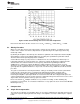
For a Class AB amplifier design, bias current is chosen such that crossover distortion is minimized while
also keeping quiescent power dissipation low. Higher bias current reduces harmonic distortion levels at
the cost of increased power dissipation. At some point there is little reduction with increased bias current
and resulting power dissipation. A tradeoff in the bias current level must be made between THD
performance and power dissipation.
MOSFET output stages typically need higher bias current than BJT output stages for good performance in
a Class AB amplifier design. What amount of bias current each solution’s output stage will require
depends completely on the user’s specific tastes and/or target specifications. Shown in Table 5 are
THD+N measurements with a 1kHz signal at 10W into 8Ω load with a 22kHz measurement bandwidth at
different total supply current settings. The LM49830 current is approximately 25mA so the output stage
bias current is equal to the total supply current minus 25mA.
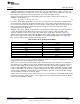
Table 5. Bias Current And Measured THD+N
Supply Current per Supply 1kHz THD+N at 10W/8Ω, 22kHz BW
50mA 0.00364%
100mA 0.00176%
150mA 0.00120%
200mA 0.00089%
250mA 0.00078%
300mA 0.00070%
500mA 0.00067%
1A 0.00067%
Table 5 indicates that the a range of 200mA to 300mA of supply current per power supply produces low
magnitude harmonics and manageable power dissipation.
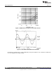
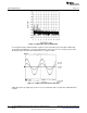
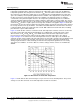
Different bias current levels are shown in the graphs and oscilloscope photos below. For each graph the
output power level is 10W into an 8Ω resistive load with 1kHz signal. Each oscilloscope photo shows the
input and output signal plus the time domain distortion residual. The measurement equipment is set to
notch out the fundamental frequency of the test signal. The fundamental is reduced by more than -110dB
relative to 0dB. 0dB is set equal to the voltage for 10W into 8Ω. The graphs show how an insufficient bias
current results in THD that is dominated by crossover distortion. Under bias is also indicated by the high
level and number of harmonics in the FFT graphs.
THD+N curves over frequency representing the level of crossover distortion associated with varying output
stage bias currents are shown in Figure 8. The output power level is 10W into an 8Ω load with an 80kHz
measurement bandwidth for all plots.
13
SNAA058B–July 2008–Revised May 2013 AN-1850 LME49830TB Ultra-High Fidelity High-Power Amplifier Reference
Design
Submit Documentation Feedback
Copyright © 2008–2013, Texas Instruments Incorporated