
Specifications


www.ti.com
Operational Details
Table 1. Output Power Levels
Load 0.1% THD+N 1% THD+N 10% THD+N
4Ω 335W 350W 430W
8Ω 175W 185W 230W
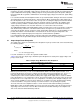
Figure 3. LME49830 EF125WT1 FET PCB Amplifier Schematic
It is important to note that the LME49830 EF125WT1 FET PCB amplifier module contains no output stage
protection mechanisms. A proper current limit set on the evaluation power supply is the minimum
precaution for safety.
The power supply voltage limitation for the EF125WT1 FET module is based on the Toshiba
2SK1530/2SJ201 MOSFET devices, which have a V
DSS
of 200V as well as the LME49830 which has an
absolute maximum supply voltage rating of ±100V (200V). Based on this, it is recommended that the
maximum power supply voltage applied to the amplifier module be less than ±80V. To allow for additional
safety margin it is recommended that the maximum power supply voltage is ±75V.
While power supply voltages up to ±75V can be applied to the amplifier module, it is recommended that
caution be applied when driving a load with an impedance less than 8Ω with continuous sinusoidal
signals. Only two output power transistors per side with limited power dissipation capabilities on the
provided heat sink does not allow for continuous total output stage power dissipation levels above 140W
with only convection cooling. The amplifier module’s limiting factor is the output stage power transistor
5
SNAA058B–July 2008–Revised May 2013 AN-1850 LME49830TB Ultra-High Fidelity High-Power Amplifier Reference
Design
Submit Documentation Feedback
Copyright © 2008–2013, Texas Instruments Incorporated