
User Guide

BIOS Setup 3-15
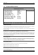
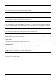
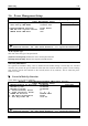
3-4. Advanced Chipset Features
Phoenix – Award WorkstationBIOS CMOS Setup Utility
Advanced Chipset Features
► DRAM Configuration Press Enter Item Help
► LDT & PCI Bus Control Press Enter
Dual Slot Configuration Disabled
X GFX1 Link Width X8
GFX0 Link Width X16
Memory Hole Disabled
Init Display First PCIEx
System BIOS Cacheable Disabled
↑↓:Move Enter:Select +/-/PU/PD:Value F10:Save ESC:Exit F1:General Help
F5: Previous Values F6: Fail-Safe Defaults F7: Optimized Defaults
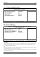
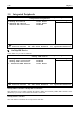
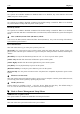
# DRAM Configuration:
Click <Enter> key to enter its submenu:
Phoenix – Award WorkstationBIOS CMOS Setup Utility
DRAM Configuration
Timing Mode Auto Item Help
X Memclock index value (Mhz) 200Mhz
X CAS latency (Tcl) 2.5
Bottom of 32-bit[31:24] IO D8
S/W memory hole Remapping Disabled
H/W memory hole Remapping Disabled
MTRR mapping mode Continuous
↑↓:Move Enter:Select +/-/PU/PD:Value F10:Save ESC:Exit F1:General Help
F5: Previous Values F6: Fail-Safe Defaults F7: Optimized Defaults
Timing Mode:
This item selects the DRAM timing mode. When set to “By SPD”, the BIOS will read the DRAM module
SPD data and automatically set to the values stored in it. Leave this item to its default “Auto” setting.
! Memclock index value (Mhz):
This item sets the DRAM clock of your DRAM module. The system may be unstable or unable to boot up
if your DRAM module does not support the clock you set.
When set to [By SPD], the BIOS will read the DRAM module SPD data and automatically set the DRAM
clock by the value stored in it.
User’s Manual