
Product Info


ABLUE TECHNOLOGY
COPYRIGHT ©2020 ALL RIGHTS RESERVED ABLUE Technology E-mail: info@abluetech.com
4
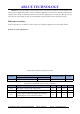
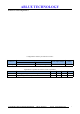
Pin
Name
Description
Recommend usage
Pin1
P0.17
Digital I/O
Standard drive, low frequency I/O
Pin2
P0.18/RESET
Digital I/O/ RESET
Pin3
P0.16
Digital I/O
Standard drive, low frequency I/O
Pin4
P0.20
Digital I/O
Pin5
SWDCLK
HW debug and programming
Pin6
SWDIO
HW debug and programming
Pin7
P0.15
Digital I/O
Pin8
P0.14
Digital I/O
Pin9
P0.07
Digital I/O
Pin10
D+
USB D+
USB
Pin11
D-
USB D-
USB
Pin12
VBUS
USB Power
5 V input for USB 3.3 V regulator
Pin13
VDDH
High voltage power supply
Pin14
P0.06
Digital I/O
Pin15
P0.05/AIN3
Digital I/O/Analog input 3
Pin16
P0.01/XL2
Reserve for 32.768KHz use
Pin17
P0.00/XL1
Reserve for 32.768KHz use
Pin18
P0.04/AIN2
Digital I/O/Analog input 2
Pin19
P0.02/AIN0
Digital I/O/Analog input 0
Pin20
P0.03/AIN1
Digital I/O/Analog input 1
Standard drive, low frequency I/O
Pin21
P0.28
Digital I/O
Standard drive, low frequency I/O
Pin22
P0.30
Digital I/O
Standard drive, low frequency I/O
Pin23
VDD
Power Supply
Pin24
GND
Ground
Pin25
P0.29
Digital I/O
Standard drive, low frequency I/O
Pin26
P0.08
Digital I/O
Standard drive, low frequency I/O
*Low frequency I/O is signals with a frequency up to 10 kHz
*Internal 32.768 kHz RC oscillator is used to provide low frequency clock by default. If you want to use an
external crystal, you can use the reserved pins (Pin16 and Pin17) to connect the external crystal and modify the
firmware configuration.
Note: An internal 4.7μF bulk capacitor has been included on the module. For those application that with heavy
GPIO usage and/or current draw, it is good design practice to add additional bulk capacitance as required for
your application.
General Purpose I/O:
Each GPIO can be accessed individually with the following user configurable features:
Input/output direction
Output drive strength
Internal pull-up and pull-down resistors
Wake-up from high or low level triggers on all pins
Trigger interrupt on all pins