
Product Info


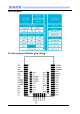


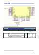


Table Of Contents

COPYRIGHT ©2019 ALL RIGHTS RESERVED XUNTONG Tech E-mail: nrf@freqchina.com
6
Pin
Flash Program interface
SWDIO
Debug and flash programming I/O
SWDCLK
Debug and flash programming I/O
This is the hardware debug and flash programming of module, J-Link Lite support, please refer
www.segger.com
.
Power and Configuration:
The module has two internal regulator stages. REG1 regulator stage has the regulator type
options of Low-dropout regulator (LDO) and Buck regulator (DC/DC). REG0 regulator stage has only
the option of Low-dropout regulator (LDO). The first regulator, REG0, is fed by the VDDH pin and can
accept a source voltage of 2.5 V to 5.5 V. The output of REG0 is connected to the VDD pin and the
input of the second regulator stage REG1. REG1 supplies power to the module core and can accept
an input source voltage of 1.7V to 3.6V. Depending on how the VDD and VDDH pins are connected,
the module will operate in one of two modes: Normal/Low Voltage (LV) or High Voltage (HV). The
voltage present on the VDD pin is always the GPIO high logic level voltage, regardless of power
mode.
To enter LV Mode, the same source voltage is applied to both the VDD and VDDH pins causing
REG0 to automatically shut down leaving only the REG1 stage active. To enter HV, the source voltage
is only applied to VDDH causing the VDD pin to become an output source supplied by REG0.
Mode
Pin of
Module
Name
Power Connection
Normal/Low Voltage
(LV)
Pin 34
VDD
1.7V to 3.6V source in
Pin 46
VDDH
Same source as VDD
High Voltage (HV)
Pin 34
VDD
1.8V to 3.3V supply out
Pin 46
VDDH
2.5V to 5.5V source in
Im
portant: In both LV and HV modes, the GPIO logic level voltage is determined by the VDD pin.
In HV mode, all external devices that are connected to the Module’s GPIO must either be powered by
the module (from VDD) or use level translation.
RE
G0 can supply a maximum current of 25mA for the module and external circuits in System On
Mode and 1 mA in System Off Mode. External circuits powered from VDD in HV mode should be
limited to no more than 5 mA to ensure stability at all radio transmit power levels.
USB
Power: The USB interface on the Module can be used when the module is in either Normal
/Low Voltage (LV) or High Voltage (HV) mode. The Module USB PHY is powered by a dedicated,
internal LDO regulator that is fed by the VBUS pin (Pin43). This means that applying power to only the
VBUS pin will not power the rest of the module. In order for the USB PHY to operate, VBUS must be
externally powered.