0623 Roselle Street, San Diego, CA 92121 • (858) 550-9559 • FAX (858) 550-7322 contactus@accesio.com • www.accesio.com MODEL PCI-DIO-24D(H) USER MANUAL FILE: MPCI-DIO-24DH.
Notice The information in this document is provided for reference only. ACCES does not assume any liability arising out of the application or use of the information or products described herein. This document may contain or reference information and products protected by copyrights or patents and does not convey any license under the patent rights of ACCES, nor the rights of others. IBM PC, PC/XT, and PC/AT are registered trademarks of the International Business Machines Corporation. Printed in USA.
Warranty Prior to shipment, ACCES equipment is thoroughly inspected and tested to applicable specifications. However, should equipment failure occur, ACCES assures its customers that prompt service and support will be available. All equipment originally manufactured by ACCES which is found to be defective will be repaired or replaced subject to the following considerations. Terms and Conditions If a unit is suspected of failure, contact ACCES' Customer Service department.
Table of Contents Chapter 1: Introduction................................................................................................. 5 Specifications ............................................................................................................ 7 Figure 1-1: Card D or H Block Diagram .................................................................. 8 Chapter 2: Installation.................................................................................................
Chapter 1: Introduction Features • 24 Bits of Digital Input/Output. • All 24 I/O Lines Buffered on the Card. • I/O Buffers Can Be Tri-stated under Program Control. • Four and Eight Bit Ports Independently Selectable for I/O. • Pull-Ups on I/O Lines. Pull Down resistors may be installed at the factory (**per port 8 bit**) • Resettable fused +5V Supply Available to the User. • "H" version compatible with Industry Standard I/O Racks.
output use according to direction assignment from a control register in the PPI. Further, if a jumper is properly placed on the card, the tristate buffers may be enabled/disabled under program control. (See the Option Selection section to follow.) I/O wiring connections for the H card are via a 50-pin connector on the back plate of the card. Flat insulation-displacement ribbon cables can be used to connect these cards to termination panels and relay output cards.
Specifications Digital Inputs (TTL Compatible) • Logic High: 2.0 to 5.0 VDC • Logic Low: -0.5 to +0.8 VDC • Load: ±20 μA Digital Outputs • Logic High: 2.0 VDC min., source 32 ma • Logic Low: 0.55 VDC max., sink 64 ma Optional Counter/Timers • Type: 82C54 programmable interval counters (up to three) • Output drive: Source 2.
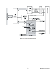
Figure 1-1: Card D or H Block Diagram 8 Manual PCI-DIO-24DH
Optional Counter/Timers These cards have options to include one, two, or three 82C54 counter(s) that each include three 16-bit counter/timers factory configured in an optimal module for use as event counters, frequency output, pulse width, and frequency measurement. See the Block Diagram which shows one 82C54 counter. If your card has one or more of these optional counters, an -S01, -S02, or -S03 is appended to the model number for one, two, or three counters respectively.
Chapter 2: Installation A printed Quick-Start Guide (QSG) is packed with the card for your convenience. If you’ve already performed the steps from the QSG, you may find this chapter to be redundant and may skip forward to begin developing your application. The software provided with this card is on CD and must be installed onto your hard disk prior to use. To do this, perform the following steps as appropriate for your operating system.
Hardware Installation 1. 2. 3. 4. 5. 6. 7. 8. 9. 10. Make sure to set switches and jumpers from either the Option Selection section of this manual or from the suggestions of SETUP.EXE. Do not install card into the computer until the software has been fully installed. Turn OFF computer power AND unplug AC power from the system. Remove the computer cover. Carefully install the card in an available 5V or 3.3V PCI expansion slot (you may need to remove a backplate first).
Chapter 3: Option Selection Refer to the setup programs on the CD provided with the card. Also, refer to the Block Diagram and the Option Selection Map when reading this section of the manual. Buffer Mode Jumper A means of enabling or disabling (tristating) the 74ABT245B input/output buffers under program control is provided at the jumper position labeled TST/BEN. When the jumper is in the BEN (Buffer Enable) position, the I/O buffers are always enabled.
4.8" IRQD INTEN IRQT 3.
Chapter 4: Address Selection These cards use one address space and occupy sixteen I/O locations. The S03 (which has 3 counters) version takes up 32 I/O locations. PCI architecture is Plug-and-Play. This means that the BIOS or Operating System determines the resources assigned to PCI cards rather than the user selecting those resources with switches or jumpers. As a result, you cannot set or change the card's base address or IRQ level. You can only determine what the system has assigned.
Chapter 5: Software There are sample programs provided with the card in C, Pascal, QuickBASIC, and several Windows languages. DOS samples are located in the DOS directory and Windows samples are located in the WIN32 directory. The following paragraphs describe the setup program and the 16- and 32-bit utility drivers. SETUP.EXE This program is supplied in the root or base directory as a tool for you to use in configuring jumpers on the card.
Chapter 6: Programming These cards are I/O-mapped devices that are easily configured from any language and any language can easily perform digital I/O through the card's ports. This is especially true if the form of the data is byte or word wide. All references to the I/O ports would be in absolute port addressing. Developing Your Application Software If you wish to gain a better understanding of the programs on diskette, then the information in the following paragraphs will be of interest to you.
These cards use an 8255-5 PPI to provide a total of 24 bits input/output capability. The card is designed to use the PPI in Mode 0 wherein: a. b. c. d. There are two 8-bit groups (A and B) and two 4-bit groups (C Hi and C Lo). Any port can be configured as an input or an output. Outputs are latched. Inputs are not latched. The PPI contains a Control Register. This write-only, 8-bit register is used to set the mode and direction of the ports. At Power-Up or Reset, all I/O lines are set as inputs.
c. d. Now, if any of the ports are to be set as outputs, you may set the values to that port with the outputs still in the tristate condition. (If all ports are to be set as inputs, this step is not necessary.) If data bit D7 is low when the control byte is written, ONLY the associated buffer controller is addressed.
Programming Example (C) The following program fragment in C language illustrates the foregoing: const BASE_ADDRESS 0x300; outportb(BASE_ADDRESS +3, 0x89); outportb(BASE_ADDRESS,0); outportb(BASE_ADDRESS+1,0); outportb(BASE_ADDRESS +3, 0x09); /*This instruction sets the mode to Mode 0, ports A and B as output, and port C as input. Since bit D7 is high, the output buffers are set to tristate condition. See item b. above.*/ /*These instructions set the initial state of ports A and B to all zeroes.
Enabling/Disabling I/O Buffers When using the tristate mode (Jumper in the TST position), the method to disable the I/O buffers involved writing a control word to the Control Register at Base Address +3. This control word was required to have bit D7 (the most significant bit) set. That meant that the PPI translated it as an "active mode set" and reset the output data latches to "zero" on all output ports and the output buffers were disabled.
Chapter 7: 8254 Counter/Timer These cards have the option of one, two, or three 82C54 counter(s) that each include three 16-bit counter/timers factory configured in an optimal module for use as event counters, frequency output, pulse width, and frequency measurement (See Block Diagram). Each counter can be programmed to any count as low as 1 or 2, and up to 65,535, depending on the mode chosen.
Counter/Timer Registers Base + 10 Write/Read: Counter#A0 When writing, this register is used to load a count value into the counter. The transfer is either a single or double byte transfer, depending on the control byte written to the counter control register at BASE ADDRESS +13. If a double byte transfer is used, then the leastsignificant byte of the 16 bit value is written first, followed by the most significant byte. When reading, the current count of the counter is read.
Programming the 8254 The counters are programmed by writing a control byte into the counter control register. Refer to the previous register map for the base addresses of the counters and the counter control register. The control byte specifies the counter to be programmed, the counter mode, the type of read/write operation, and the modulus.
Reading and Loading the Counters If you attempt to read the counters on the fly when there is a high input frequency, you will most likely get erroneous data. This is partly caused by carries rippling through the counter during the read operation. Also, the low and high bytes are read sequentially rather than simultaneously and, thus, it is possible that carries will be propagated from the low to the high byte during the read cycle.
1st Read: 2nd Read: 3rd Read: Status byte Low byte of latched data High byte of latched data After any latching operation on a counter, the contents of its hold register must be read before any subsequent latches of that counter will have any effect. If a status latch command is issued before the hold register is read, then the first read will read the status, not the latched value. 8254 Driver A simple driver is provided to perform basic counter/timer operations on this card.
Pulse Width The Pulse Width function will measure the width of an applied event from its rise to its fall (effectively one half the period). The Base Address of the card is required as input to the function. The signal should be applied to the CLOCK IN pin of the card. Software latency will be affected by the operating system and will set a limit on the precision of the measurement.
Chapter 8: Connector Pin Assignments The H card has a 50-pin connector provided on the back plate of these cards for I/O connections. The mating connector is an AMP type 1-746285-0 or equivalent. Connector pin assignments are listed below. Assignment Port C Hi Port C Lo Port B Port A Fused +5 VDC Pin Assignment Pin PC7 1 Counter A0 Freq In 2 PC6 3 Ctr A1 P.W.I. (Gate) 4 PC5 5 Counter A2 Freq Out 6 PC4 7 Counter B0 Freq in 8 PC3 9 Ctr B1 P.W.I.
The D card has a 37-pin D-sub connector provided on the back plate of these cards for I/O connections. If all three counters are present, pin 20 is counter C2's frequency output. Otherwise, pin 20 is fused +5V power.
Customer Comments If you experience any problems with this manual or just want to give us some feedback, please email us at: manuals@accesio.com. Please detail any errors you find and include your mailing address so that we can send you any manual updates. 10623 Roselle Street, San Diego CA 92121 Tel. (858)550-9559 FAX (858)550-7322 www.accesio.