
Data Sheet


A111 Pulsed Coherent Radar (PCR)
Datasheet, v2.0 prel.
© 2019 Copyright by Acconeer 2019-11-01 Page 6 of 33
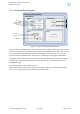
2.1 Functional Block Diagram
A111 One Package Solution
A111 Silicon
TX
RX
PLL
LDOs
PoR
Communication
Program
memory
Data
memory
SPI (4)
INTERRUPT
XIN (ref clk)
XOUT
1.8V Single
power supply
ENABLE
Digital
Power
Timing
mmWave Radio
Tx ant.
Rx ant.
Figure 2.1. The A111 functional block diagram.
The A111 silicon is divided into four functional blocks: Power, Digital, Timing and mmWave radio.
The Power functional block includes LDOs and a Power on Reset (PoR) block. Each LDO creates its
own voltage domain. The PoR block generates a Reset signal on each power-up cycle. The host
interfaces the Power functional block of the sensor via 1.8V Single power supply and ENABLE.
The Digital functional block includes sensor control. The data memory stores the radar sweep data
from the ADC. The host interfaces the Sensor via an SPI interface, a Clock (XIN, XOUT) and
INTERRUPT signal.
The Timing block includes the timing circuitry.
The mmWave radio functional block generates and receives radar pulses and includes transmitter
(TX), receiver (RX) and interfaces toward the integrated antennas.