t ne el. w.
Service Guide Version and Revision Release Date Revision History TPV model A00 Aug.-23-2008 Initial Release T8RAM5D82WABAN ht tp :// ww w. wj el.
Copyright Copyright © 2003 by Acer Incorporated. All rights reserved. No part of this publication may be reproduced, Transmitted, transcribed, stored in a retrieval system, or translated into any language or computer language, in any form or by any means, electronic, mechanical, magnetic, optical, chemical, manual or otherwise, without the prior written permission of Acer Incorporated. Disclaimer The information in this guide is subject to change without notice.
Preface Before using this information and the product it supports, please read the following general information. 1. This Service Guide provides you with all technical information relating to the BASIC CONFIGURATION decided for Acer's "global" product offering. To better fit local market requirements and enhance product competitiveness, your regional office may have decided to extend the functionality of a machine (e.g. add-on card, modem, or extra memory capability).
Precautions z Do not use the monitor near water, e.g. near a bathtub, washbowl, kitchen sink, laundry tub, swimming pool or in a wet basement. z Do not place the monitor on an unstable trolley, stand, or table. If the monitor falls, it can injure a person and cause serious damage to the appliance. Use only a trolley or stand recommended by the manufacturer or sold with the monitor. If you mount the monitor on a wall or shelf, uses a mounting kit approved by the manufacturer and follow the kit instructions.
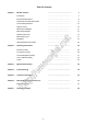
7 Introduction ……………………………………… 7 Electrical Requirements ……………………………………… 8 LCD Monitor General Specification ……………………………………… 9 LCD Panel Specification ……………………………………… 10 Support Timing ……………………………………… 12 Monitor Block Diagram ……………………………………… 13 Main Board Diagram ……………………………………… 14 Software Flow chart ……………………………………… 15 Main Board Layout ……………………………………… 17 Installation ……………………………………… 19 Attaching/Removing the base ……………………………………… 18 Operating Instructions ………………………………………
Chapter 1 Monitor Features Introduction Scope This specification defines the requirements for the 18.5” MICROPROCESSOR based Multi-mode supported high resolution color LCD monitor. This monitor can be directly connected to general 15-pin D-sub VGA connector, also supports VESA DPMS power management and plug & play function. Description The LCD monitor is designed with the latest LCD technology to provide a performance oriented product with no radiation. This will alleviate the growing health concerns.
Electrical Requirements Standard Test Conditions All tests shall be performed under the following conditions, unless otherwise specified.
LCD Monitor General Specification Active Display Area 409.8 (H) × 230.4(V) Pixel pitch 0.3(H) x 0.3(W) Contrast Ratio 1000 : 1 Response time 5ms Luminance of White 300(Typ.) cd/㎡ Separate Sync. H/V TTL H-Frequency 30kHz – 60kHz V-Frequency 40-75Hz (H)170 (V) 160(Type) Display Colors 16.7M Display mode 1366 x 768 @60Hz OFF Mode w. wj ON Mode EPA ENERGY STAR® el.
LCD Panel Specification This specification applies to the 18.5 inch-wide Color a-Si TFT-LCD Module M185XW01.The display supports the WXGA - 1366(H) x 768(V) screen format and 16.7M colors (RGB 6-bits + Hi-FRC data). All input signals are 1-channel LVDS interface and this module doesn’t contain an inverter board for backlight. ht tp :// Function Block Diagram ww w. wj el.
ne t Electrical Characteristics ht tp :// ww w. wj el.
ww :// tp ht ne el. w.
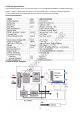
Monitor Block Diagram The LCD MONITOR will contain a main board, a power board, an audio board and a key board which house the flat panel control logic, brightness control logic and DDC. The power board will provide AC to DC Inverter voltage to drive the backlight of panel and the main board chips each voltage. Main Board AC-IN 90V-264V el. ne Inverter Board (include adapter) t Flat Panel and CCFL backlight CCFL Drive. Key board ht tp :// ww w.
Main Board Diagram Crystal (X401) 14.31818MHZ LCD Interface (CN403) (U401) ne (Include MCU ,ADC, OSD) Power Board (CN404) t Scalar IC TSUM1PFR-LF w. wj el.
Software Flow Chart 1 Y 2 3 N N 4 N ne t 5 Y el. 6 w.
Remark: 1) MCU initializes. 2) Is the EEPROM blank? 3) Program the EEPROM by default values. 4) Get the PWM value of brightness from EEPROM. 5) Is the power key pressed? t 6) Clear all global flags. ne 7) Are the AUTO and SELECT keys pressed? el. 8) Enter factory mode. 9) Save the power key status into EEPROM. Scalar initializes. 10) In standby mode? 11) Update the lifetime of back light. w. wj Turn on the LED and set it to green color.
ht tp :// ww w. wj el. ne t Main Board Layout Symbol Description Symbol Description U401 IC TSUM1PFR-LF CN401 WAFER 6PIN U404 IC AP1117D33L-13 TO252-3L DIODES CN404 WAFER 9P RIGHT ANELE PITCH U103 IC AZC099-04S SOT23-6L CN403 CONNECTOR U102 IC AZC099-04S SOT23-6L X401 U402 SST25VF010A-33-4C-SAE CN101 17 14.
Installation To install the monitor on your host system, please follow the steps below: Steps 1 Connect the video cable A:Make sure both the monitor and computer are switched off. B:Connect the VGA video cable to the computer. 2 Connect the power cord Connect the power cord to the monitor, then to a properly grounded AC outlet. 3 Turn on the monitor and computer Turn on the monitor first, then the computer. This sequence is very important. ht tp :// ww w. wj el.
Attaching/Removing the Base Attaching: Align the release button on the bottom of the monitor with the corresponding slots on the bottom of the base. Removing: ht tp :// ww w. wj el. ne t Press the release button as indicated, then pull in the direction of the arrow to remove the base.
Chapter 2 Operating Instructions Press the power button to turn the monitor on or off. The other control buttons are located at front panel of the monitor. By changing these settings, the picture can be adjusted to your personal preferences. • The power cord should be connected. • Connect the video cable from the monitor to the video card. • Press the power button to turn on the monitor position. The power indicator will light up. w. wj el. ne t External Controls Front panel controls 1.
ht tp :// ww w. wj el.
ht tp :// ww w. wj el.
ht tp :// ww w. wj el.
ww :// tp ht ne el. w.
Logo When the monitor is power on, the LOGO will be showed in the center, and disappear slowly. How To Optimize The DOS-Mode Plug And Play Plug & Play DDC2B Feature This monitor is equipped with VESA DDC2B capabilities according to the VESA DDC STANDARD. It allows the t monitor to inform the host system of its identity and, depending on the level of DDC used, communicate additional ne information about its display capabilities. el. The DDC2B is a bi-directional data channel based on the I²C protocol.
Chapter 3 Machine Disassembly This chapter contains step-by-step procedures on how to disassemble the monitor for maintenance. Disassembly Procedure Fig 1 el. ne t 1. Remove the cover hinge as the following indicator. (Fig 1) ht tp :// ww w. wj 2. Remove the screws as following indicate to release base stand.
tp :// ww el. w. wj Fig 3 ne t Remove the back cover and bezel. (Fig 3,4) ht 3.
4. Remove the lamp connectors and remove the screws to remove the panel. Put attention to the LVDS cable. (Fig 5,6) w. wj el. ne t Fig 5 Fig 6 tp :// ww Remove the screws to remove the main board and power board.( Fig 7,8) ht 5.
ww :// tp ht ne el. w.
Chapter 4 Troubleshooting This chapter provides troubleshooting information for the X193HQ: 1. No Power No power Press power key and look if the picture is normal t NG el. NG Reinsert or check the power section w. wj OK ne Please reinsert and make sure the AC of 100-240 is normal Measure U404 Pin2=3.
2. No Picture (LED is orange) No picture NG The button if under control X401 oscillate waveform is normal NG Replace X401 OK OK Check reset circuit of U401 is normal NG Check Correspondent component Measure U404 Pin2=3.3V, Replace U401 el. OK NG w.
3. Panel Power Circuit White screen NG Measure Q404 base is low level? X401 oscillate waveform is normal OK NG Replace X401 ne t OK Check CN403 is solder and Q404,Q405 is OK? el. NG NG w. wj Check Correspondent component. Check reset circuit of U401 is normal OK OK ht tp :// ww Replace PANEL Replace U401 32 Check Correspondent component.
4. Key Board OSD is unstable or not working NG Connect Key Board Is Key Pad Board connecting normally? Y ne el. Y NG ht tp :// ww Check Main Board Replace Key Board w.
5. Power Board 1) No power Check CN902 pin4, 5 = 12V NG Check AC line volt 110V or 220V NG Check AC input ne t OK Check the voltage of C905(+) NG Check bridge rectified circuit and F901 circut el. OK NG Check R904, R932, R933, and Change IC901 ww OK w.
2.) No Backlight Check CN902 pin4, 5 = 12V NG OK Check the adapter and F801 Check ON/OFF signal and the pin 12 of IC801 is 12V NG OK Check main board or change ON/OFF signal ne t Check the pin5 of IC801 have saw tooth wave NG OK el. Change IC801 NG OK w. wj Check the PWM wave from the pin9,10 of IC801 ww Check IC801 Check Q802 PIN5, 6, 7, 8 have the output NG of square wave at short time.
Chapter 5 Connector Information ht tp :// ww w. wj el.
Chapter 6 FRU (Field Replaceable Unit) List This chapter gives you the FRU (Field Replaceable Unit) listing in global configurations of X193HQ. Refer to this chapter whenever ordering for parts to repair or for RMA (Return Merchandise Authorization). NOTE: Please note WHEN ORDERING FRU PARTS, that you should check the most up-to-date information available on your regional web or channel (http://aicsl.acer.com.tw/spl/).
Part List Above picture show the description of the following component. Item Picture Description Main Frame ww w. wj el.
4 el. ne t Power Board Main Board tp Audio Board ht 6 :// ww w.
Chapter 7 Schematic Diagram Main Board H_Sy nc V_Sy nc R101 0R05 1/10W 5% DSUB_SDA 12 11 DSUB_5V ZD103 UDZSNP5.6B FB103 VGA_G+ DB15 1 Connect Pin4 and Pin11 of CN101 to GND to prevent ESD issue. .w j 75R 1/16W 5% DGND ESD_VCC 1 75R 1/16W 5% ESD_VCC U103 DSUB_SDA DSUB_SCL 1 2 3 I/O1 I/O4 GNDVDD I/O2 I/O3 6 5 4 H_Sy nc V_Sy nc C115 NC AZC099-04S 候綼 U1 03 U102 VGA_R+ 1 2 3 I/O1 I/O4 GNDVDD I/O2 I/O3 AZC099-04S ESD_VCC 6 5 4 VGA_B+ C114 NC 候綼 U1 01 DSUB_R+ 5 DSUB_R- 5 0.
AVDD VDDP VDDC RIN0P RIN0M GIN0P GIN0M SOGIN0 BIN0P BIN0M HSY NC0 VSY NC0 DDCA_SDA/RS232_TX DDCA_SCL/rs232_RX 30 53 51 7 VDDC VDDC VDDP 13 12 10 9 11 8 7 16 17 18 19 DSUB_R+ DSUB_RDSUB_G+ DSUB_GDSUB_SOG DSUB_B+ DSUB_BDSUB_H DSUB_V DDC1_SDA DDC1_SCL AVDD_ADC 3 3 3 3 3 3 3 3 3 3 3 6 VCC3.3 U401 VCTRL LVA3P LVA3M LVA2P LVA2M LVA1P LVA1M LVA0P LVA0M 52 33 34 35 36 37 38 39 40 VCTRL VDDP 7 PA0 PA1 PA[0..1] PA4 PA5 PA6 PA7 PA8 PA9 PA[0..1] 300OHM C403 C404 0.1uF/16V 0.1uF/16V 5 VCC1.
CN403 change to 14P Dip connector based on 715G2904-D CN403 5 PB[0..9] PA0 PA1 5 PA[4..9] PA[4..9] PA4 PA5 PA6 PA7 PA8 PA9 VCC3.3 R443 0R05 1/16W NC/0ohm VCC3.38 C419 10K 1/16W 5% 0.1uF/16V Q404 PMBS3906 LVB0M LVB1M LVB2M LVBCKM LVB3M CONN PANEL_VCC 2 S R434 AO3401L 330 OHM 1/4W C420 0.
2008/01/14 BAT99 : If 0.05A,VF=1.0V BAV70 : If 0.05A,VF=1.0V It's need to use Low Dropout Regulator. ESD_5V ESD_5V 5 DSUB_5V OTHER CMVCC1 CMVCC1 NC NC(R0402) 5 PANEL_ID# 5 NC C425 Mute R439 10K 1/16W 5% 10K 1/16W 5% BKLT-EN R449 5 on_BACKLIGHT R440 4K7 1/16W 5% R446 NC R441 Volume 1K 1/16W 5% VCC3.3 5 VCC1.8 Q409 KN2907AS VCTRL MVCC Volume# C432 FB403 5 + C423 0.1uF/16V 100uF25V NC VCC3.3 10K 1/16W 5% :// w 5 VCC1.
Power board 1 2 3 4 6 4 R909 10R 1/4W 11 R962 100 6 1 8 R933 4K7 1/4W Vcc DRAIN GND HVS PROTECT DRIVER CTRL SENSE R907 NC 8 7 6 5 FB901 BEAD 3 12 D903 IN4148W Q901 STP10NK70ZFP 3 4 R915 220K 1/8W ! FG L901 R910 R938 10R 1/4W 10K 1/8W R917 1K 1/8W R912 22K 1% 1/8W ! R913 NC R911 1K 1/8W 2 R916 1K5 1/8W 4.0mH ! R901 1/4W 680K ! 1/4W ! ! ! F901 4A/250V 3 t NR901 NTCR 2 SOCKET FG R914 0.27 2W C928 0.0012uF C921 0.
E C803 1000pF 1 2 R812 33 1/4W F801 0 OHM 1/4W +12V 3.6K R804 100 1/8W R806 1% 1/10W C802 470UF/25V Q801 PMBS3904 R809 3.6K C824 0.1uF + 1% 1/10W 4 2 Q804 PMBS3906 1 ON/OFF 2 Q805 PDTC144WK 1 R839 22R 1/8W B 4 3 5 D805 BAW56 1 R817 10K 1/10W R821 1K 1/10W 1% 3 C801 15pF/6KV 6 7 CN801 CONN 2 C819 0.01uF 1 R801 1K5 1/10W 1% 9 S D G D S D 6 7 D801 BAV99 C839 1000pF 2 1 R828 10K 1/10W 8 R822 1K 1/10W 1% ne t 3 C823 0.01uF Q811 PMBS3904 CN802 CONN 3 .
Audio board CN602 1 2 3 4 5 6 7 8 9 10 11 12 CN602 NC NC 1 CN603 CN605 GND VOL MUTE NC RR+ LL+ CONN CN604 C603 4 5 14 GND R603 R607 :// w 22K OHM 18 10K OHM 0.001uF GND 6 GND VDD LIN- LOUT- RIN+ ROUT+ + C609 1uF50V RIN- ROUTBY PASS SHUTDOWN# FADE# SE/BTL# VOLUME 1 0.001uF LOUT+ NC PGND R611 10K OHM R606 22K OHM C611 LIN+ PGND GND GND + C604 100uF/16V GND 12 10 20 2 16 15 + 19 C608 1uF50V GND 13 AGND 7 ww C607 0.47UF25V 8 17 C606 0.
Key board LED001 LED 1 GND 0.65V ECOLOR(GND) 0 V AUTO 3 5 4 GND change Net name MENU--->AUTO AUTO----MENU CN001 CONNECTOR ECOLOR AUTO MENU VOL- GND1 GND2 GND-EMI GND-EMI GND VOL+ POWER LED TPV ( Top Victory Electronics Key Component Date 47 Co . , Ltd. ) OEM MODEL TPV MODEL 絬隔瓜絪腹 02.Key Board Sunday , June 17, 2007 Size ACER Rev PCB NAME Sheet 1 of 2 称爹 B A <称爹> ZD005 2 C006 SW005 SW NC ZD002 1 UDZS5.6B 4 C008 5 2007/5/18 NC 3 2 UDZS5.