Speedster22i PCIExpress User Guide UG030, April 26, 2013 UG030, April 26, 2013 1
Copyright Info Copyright © 2013 Achronix Semiconductor Corporation. All rights reserved. Achronix is a trademark and Speedster is a registered trademark of Achronix Semiconductor Corporation. All other trademarks are the property of their prospective owners. All specifications subject to change without notice. NOTICE of DISCLAIMER: The information given in this document is believed to be accurate and reliable.
Table of Contents Copyright Info .................................................................................. 2 Table of Contents ............................................................................ 3 Table of Figures .............................................................................. 5 Introduction ..................................................................................... 6 Design Overview .............................................................................
Appendix C: Maximum Supported Clock Frequencies............... 80 Revision History ..............................................................................................
Table of Figures Figure 1: PCIe with DMA Block Diagram .......................................................................... 8 Figure 2: DMA Block Diagram ........................................................................................... 9 Figure 3: AXI Target Interface .......................................................................................... 10 Figure 4: Timing Diagram for Target Interface ...............................................................
Introduction The Achronix PCI Express (PCIe) hard core provides a flexible and high-performance Transaction Layer Interface to the PCIe Bus for the Speedster22i device. The core implements all three layers (Physical, Data Link, and Transaction) defined by the PCIe standard, as well as a high-performance DMA interface to facilitate efficient data transfer between the PCIe Bus and user logic. The core is available in numerous configurations including x16, x8, x4, x2, and x1 Lanes.
o Decodes received packets to provide key routing (BAR hits, Tag, etc.
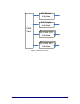
Design Overview The PCI Express (PCIe) standard can be implemented in the Achronix22i device. Figure 1 shows a block diagram of the PCIe hard IP with the DMA core for high-speed data transfer to/from the user fabric. Figure 2 shows the DMA’s major interfaces, which will be discussed later.
AXI Master Interface AXI Target Interface DMA Core AXI DMA C2S Interface AXI DMA S2C Interface Figure 2: DMA Block Diagram UG030, April 26, 2013 9
Major Interfaces AXI Target Interface The AXI Target Interface implements AXI3/AXI4 Master Protocol. Write and read requests received via PCI Express (from remote PCI Express masters) that target AXI regions of enabled Base Address or Expansion ROM regions are forwarded to the AXI Target Interface for completion. Accesses to registers inside the AXI DMA Back-End Core are handled by the core and do not appear on the AXI Target Interface.
Ordering is maintained separately for internal DMA Register and AXI destinations The completion of a read request to the same destination (DMA Registers or AXI) can be used to guarantee that prior writes to the same destination have completed Reads are blocked until all writes occurring before the read have fully completed; for AXI, a write is completed when it returns a completion response on the Write Response Channel; for internal DMA Registers, a write is completed when it is written into the DMA
... t_areset_n St1 t_aclk St1 ... t_awvalid St0 ... t_awready St1 ... t_awregion[2:0] 3'h0 t_awaddr[31:0] ... t_awlen[3:0] 4'h0 t_awsize[2:0] 3'h4 ... 0 ... 31ff 808c 0 ... 0 4 ... 4 0 * 8080 31ff 8084 31ff 8088 t_wvalid St0 ... t_wready St0 ... t_wdata[127:0] ... t_wstrb[15:0] ... t_wlast St1 t_bvalid St0 t_bready St1 t_bresp[1:0] 2'h0 t_arvalid St0 t_arready St0 00 0000 0000 * aea1 0001 0000 0000 000f * 0002 0000 0000 00f0 ... ... ... 0 ... ..
synchronization techniques can be used to enable support for a wide variety of AXI clock rates. User’s Task: It is important to consume target write and read transactions relatively quickly as it is possible to stall PCI Express completions (used for S2C DMA for example) if target write and read transactions are allowed to languish in the PCI Express Core Receive Buffer.
transactions for this packet. This allows the user hardware design to implement FIFOs for some AXI DMA transactions while simultaneously also supporting addressable RAM for other AXI DMA transactions. Figure 5 depicts the Card-to-System DMA interface and Figure 6 the System-to-Card DMA interface.
... ... s2c_areset_n[1:0] 2'h3 s2c_aclk[1:0] 2'h0 ... ... s2c_aclk[1] St0 ... ... s2c_aclk[0] St0 ... ... s2c_fifo_addr_n[1:0] 2'h3 s2c_awvalid[1:0] 2'h0 3 3 ... 3 0 0 3 ... 0 0 ... 3 ... 0 s2c_awvalid[1] St0 ... ... s2c_awvalid[0] St0 ... ... s2c_awready[1:0] 2'h3 ... s2c_awready[71:0] ... 7b00 00 0000 ... ... 3 0001 7c00 3 00 0000 0000 0001 7d00 ... 00 0000 0000 0001 7d00 8'h0f 0f ... 0f ... 0f 2'h0 0 ... 0 ...
Control portion of the Descriptor. Status fields indicate to software the Descriptor completion status. Software should zero all status fields prior to making the Descriptor available to the DMA Engine. To promote ease of re-using Descriptors (for circular queues), Control and Status fields are assigned their own locations in the Descriptor. Table 1 described the Packet DMA Descriptor format.
UG030, April 26, 2013 C2SDescControlFlags[7:0] – Control • Bit 7 – SOP – Set if this Descriptor contains the start of a packet; clear otherwise; only set for addressable Packet DMA • Bit 6 – EOP – Set if this Descriptor contains the end of a packet; clear otherwise; only set for addressable Packet DMA • Bits[5:3] – Reserved • Bit[2] – Addressable FIFO DMA – If set to 1, the DMA BackEnd will use the same Card Starting Address for all DMA Interface transactions for this Descriptor; this bit must be
the packet ended before filling the entire Descriptor, then C2SDescByteCount will be less than the Descriptor size DescByteCount. The received packet size is the sum of the C2SDescByteCount fields for all Descriptors that are part of a packet. • C2SDescByteCount is 20-bits so supports Descriptors up to 2^20-1 bytes. Note that since packets can span multiple Descriptors, packets may be significantly larger than the Descriptor size limit.
UG030, April 26, 2013 Bit[2] – Addressable FIFO DMA – If set to 1, the DMA BackEnd will use the same Card Starting Address for all DMA Interface transactions for this Descriptor; this bit must be set the same for all Descriptors that are part of the same packet transfer; Addressable FIFO AXI addresses must be chosen by the user design such that they are aligned to AXI max burst size * AXI data width address boundaries; For example: 16 * 16 == 256 bytes for AXI3 max burst size == 16 and AXI_D
• • • Control - During packet to Descriptor mapping, software writes the number of bytes that it wrote into the Descriptor into S2CDescByteCount. If EOP=0, then S2CDescByteCount must be the same as the Descriptor size DescByteCount. If EOP=1 and the packet ends before filling the entire Descriptor, then S2CDescByteCount is less than the Descriptor size DescByteCount.
completes. Writes perform reasonably well in either case since writes are always posted and software will generally not block on write transactions. In the Target with Master DMA design each of the three interfaces (external SDRAM, internal SRAM, and DMA registers/General Purpose I/O) are assigned a memory Base Address Register.
DMA Bypass Interface The bypass interface disables DMA backend, and communicates directly to the PCI Express core. In its place, the user can build a soft DMA engine that connects to this interface. Transmit Interface The Transmit Interface is the mechanism with which the user transmits PCIe transaction-layer packets (TLPs) over the PCI Express bus.
Receive Interface The Receive Interface is the mechanism with which the user receives PCIe packets from the PCIe bus. Packets are received and presented on the interface in the same format defined in the PCI Express Specification; the user receives complete Transaction Layer packets comprised of packet header, data payload, and optional TLP Digest.
Port List SerDes Interface Table 2: SerDes Interface Pin Descriptions Pin Name pcie_refclk_p[7:0] pcie_refclk_n[7:0] tx_p[7:0] tx_n[7:0] rx_p[7:0] rx_n[7:0] i_serdes_sbus_req [7:0] i_serdes_sbus_data [15:0] o_serdes_sbus_data [15:0] o_serdes_sbus_ack [7:0] UG030, April 26, 2013 Direction Input Input Output Output Input Input Input Input Output Output Clock i_sbus_clk i_sbus_clk i_sbus_clk i_sbus_clk Description Reference Clock Input Reference Clock Input Serial Transmit Serial Transmit Serial Receive S
Fabric-Side Interface Table 3: Fabric-Side Port Descriptions Port Name Direction Clock Description perst_n Input user_clk clk_out Output core_clk Fundamental Reset; active-low asynchronous assert, synchronous de-assert; resets the entire core except for Configuration Registers which are defined by PCI Express to be unaffected by fundamental reset; on rst_n de-assertion the core starts in the Detect Quiet Link Training and Status State Machine (LTSSM) state with the Physical Layer down (mgmt_pl_lin
Port Name i_sbus_clk i_sbus_req i_sbus_sw_rst i_sbus_data[1:0] o_sbus_ack o_sbus_rdata[1:0] bypass_clk bypass_rst_n bypass_tx_valid bypass_tx_ready bypass_tx_almost_full bypass_tx_sop Direction Clock Input Input Input Input Output Output Input Input Input Output Output Input i_sbus_clk i_sbus_clk i_sbus_clk i_sbus_clk i_sbus_clk i_sbus_clk bypass_clk bypass_clk bypass_clk bypass_clk bypass_clk bypass_clk bypass_tx_eop Input bypass_clk bypass_tx_data[127:0] Input bypass_clk UG030, April 26, 2013
Port Name bypass_tx_data_valid[15:0] bypass_tx_np_ok Direction Input Output Clock bypass_clk bypass_clk Description functionality. PCI Express Packets are integer multiples of 32-bits in length. Thus, 64-bit and 128-bit Core Data Width cores may have an unused remainder portion in the final data word of a packet.
Port Name Direction Clock bypass_rx_valid bypass_rx_ready bypass_rx_data[127:0] Output Input Output bypass_clk bypass_clk bypass_clk bypass_rx_data_valid[15:0] bypass_rx_sop Output Output bypass_clk bypass_clk UG030, April 26, 2013 Description User’s task: User logic must stop the transmission of new Non-Posted requests when vc0_tx_np_ok == 0. A non-posted packet transmission that has already asserted vc0_tx_sop must continue to be transmitted in full.
Port Name Direction Clock bypass_rx_eop Output bypass_clk bypass_rx_ecrc_error Output bypass_clk bypass_rx_decode_info[12:0] Output bypass_clk UG030, April 26, 2013 Description vc0_rx_sop is asserted, the user may assert vc0_rx_en as desired to consume the TLP. End of TLP indicator; set == 1 coincident with the last vc0_rx_data word in each packet. ECRC error indicator; set == 1 from vc0_rx_sop to vc0_rx_eop inclusive for received TLPs which contain a detected ECRC error. Clear == 0 otherwise.
Port Name Direction Clock Description UG030, April 26, 2013 are decoded differently for Completion versus Base Address Region hits Bits[8:0] – o If Completion TLP (Bit[9] == 1) Bits[8] - Reserved Bits[7:0] – Tag; the Requestor Tag contained in the TLP; use to route completions to the associated requestor logic; this field is reserved if the TLP is a message rather than a completion o If Base Address Region TLP (Bit[9] == 0) Bit[8] – When (1), the packet is a “write” transaction; when (0), the
Port Name bypass_interrupt Direction Input Clock bypass_clk Description targets Base Address Region 1 Bit[0] – (1) if the TLP targets Base Address Region 0 vc0_rx_cmd_data is valid for the entire packet (from vc0_rx_sop == 1 through vc0_rx_eop == vc0_rx_en == 1) mgmt_interrupt is used to generate interrupt events on the PCI Express link. Interrupt support is enabled by setting mgmt_cfg_constants[128] (Interrupt Enable) == 1.
Port Name Direction Clock Description mgmt_cfg_status[1183] (MSI-X Enable): MSI-X_Enable==1 : MSI-X Interrupt Mode MSI_Enable ==1 : MSI Interrupt Mode MSI-X_Enable == 0 & MSI_Enable == 0 : Legacy Interrupt Mode Note: It is illegal for software to set both MSIX_Enable and MSI_Enable at the same time.
Port Name Direction Clock Description should be ORed together onto mgmt_interrupt. 0 to 1 transition events which occur too close together to be independently transmitted are merged together into one MSI message.
Port Name Direction Clock Description set to 1 and mgmt_interrupt_msix_vector indicates the interrupt vector that is to be transmitted. Once mgmt_interrupt_msix_req is set, mgmt_interrupt_msix_req and mgmt_interrupt_msix_vector must remain at their same values until mgmt_interrupt_msix_ack is asserted == 1 indicating that the requested interrupt message was transmitted. If MSI_En == 1, then the design is operating in MSI interrupt mode.
Port Name Direction Clock Description global Function Mask (mgmt_cfg_status[1182]) or by the per vector Mask Bit (MSI-X Table entry bit 96) then that vector is masked and cannot be requested by asserting mgmt_interrupt_msix_req until the vector is unmasked.
DMA-Side Port Descriptions AXI Target Interface Table 4: Target Interface Pin Descriptions Pin Name Direction Clock t_areset_n Input t_aclk Input t_aclk t_awvalid Output t_aclk t_awready Input t_aclk t_awregion [2:0] t_awaddr [31:0] t_awlen [3:0] t_awsize [2:0] t_wvalid t_wready t_wdata [127:0] t_wstrb [15:0] t_wlast t_bvalid t_bready t_bresp [1:0] t_arvalid t_arready t_arregion [2:0] t_araddr [31:0] Output t_aclk Output t_aclk Output t_aclk Output t_aclk Output Input Output t_aclk t_ac
Pin Name Direction Clock t_arlen [3:0] t_arsize [2:0] Output t_aclk Output t_aclk t_rvalid t_rready t_rdata [127:0] t_rresp [1:0] t_rlast Input Output Input t_aclk t_aclk t_aclk Input t_aclk Input t_aclk Description target_awregion and target_arregion indicate PCI Express Base Address Region hit information: • 0: BAR0 • 1: BAR1 • 2: BAR2 • 3: BAR3 • 4: BAR4 • 5: BAR5 • 6: Expansion ROM • 7: Reserved Read Data Channel; space is reserved in the master to receive data from all outstanding read
Pin Name m_rready m_rdata [31:0] m_rresp [1:0] m_interrupt [4:0] Direction Input Output Output Output Clock m_aclk m_aclk m_aclk m_aclk Description m_rvalid == 1 and m_rready == 1 Data read Status of read request: 0 – Successful; 1, 2,3 Error System-to-Card Engine Interface Table 6: System-to-Card Interface Port Descriptions Pin Name Direction Clock s2c_areset_n Output s2c_aclk s2c_aclk [1:0] Input s2c_aclk s2c_fifo_addr_n [1:0] Input s2c_aclk s2c_awvalid [1:0] s2c_awready [1:0] s2c_awaddr [71:
Pin Name s2c_bvalid [1:0] s2c_bready [1:0] s2c_bresp [3:0] Direction Input Output Input Clock s2c_aclk s2c_aclk s2c_aclk Description multiple AXI transfers), that provides the UserControl[63:0] value software placed in the first Descriptor of the packet.
Pin Name c2s_rvalid [1:0] c2s_rready [1:0] c2s_rdata [255:0] c2s_rresp [3:0] c2s_rlast [1:0] c2s_ruserafull [1:0] c2s_ruserstrb [31:0] Direction Clock Description Input Output Input Input Input Output c2s_aclk c2s_aclk c2s_aclk c2s_aclk c2s_aclk c2s_aclk Input c2s_aclk FIFO DMA: Read Data Channel implements AXI4Stream Slave protocol using c2s_rdata(tdata), c2s_ruserstrb(tkeep), c2s_rlast(tlast), c2s_rvalid(tvalid), and c2s_rready(tready).
Pin Name Direction pm_l1_enter Output pm_l1_exit Output pm_l2_enter Output pm_l2_enter_ack Input Clock Description useful for user designs to monitor power state changes and to determine if they want to assert a PME event to change the power state back to D0. Set to 1 by the core for 1 clock when the core begins the process of entering the L1 link state; 0 otherwise.
Pin Name Direction pm_l2_exit Output pm_l2_store[2:0] Output pm_d3cold_exit UG030, April 26, 2013 Input Clock Description PME_TO_Ack message does not arrive in a timely fashion. The PCI Specification recommends a system timeout be implemented in the 1mS to 10mS range. pm_enter_l2_ack delay should be significantly less than the system timeout (system dependent). Set to 1 by the core for 1 clock when the core exits the L2 link state back to L0; 0 otherwise.
Pin Name Direction pm_d3cold_exit_ack Output pm_d3cold_restore pm_d3cold_pme_asserted pm_d3cold_n_pme_assert Input Input Input Clock Description must be 1 if the user asserted WAKE# or generated a Beacon to wake-up the system while in D3cold and is 0 otherwise. Set to 1 for 1 clock to acknowledge pm_d3cold_exit == 1; 0 otherwise.
core_cfg_exp_addr [11:2] Input core_clk core_cfg_exp_wr_en Input core_clk core_cfg_exp_wr_data[31:0] Input core_clk Data to write to the addressed Configuration Register; must be conditionally applied using the cfg_exp_wr_be byte enables.
Appendix A: ACE PCIe Configuration GUI The Achronix Cad Environment (ACE) PCIe Configuration GUI (pci.acxip) provides a graphical and intuitive method by which the user can generate HDL files for the desired PCIe core functionality. Table 10 describes the values encountered in the GUI. Table 10: ACE PCIe GUI Field Descriptions Field Name Default Values Description System Configuration PCIe Version 3.0 UG030, April 26, 2013 1.0, 2.0, 3.0 PCIe Gen1/2/3 Verilog Parameter If(2.0 or 3.0) { If(3.
Field Name Default Values Description PCIe Width Device ID 8 0xE004 1, 4, 8 0x0000 – 0xFFFF Number of SerDes lanes PCIe Device ID Subsystem ID Revision ID 0xE004 Subsystem ID 0x04 Revision ID Vendor ID 0x19AA Vendor ID Subsystem Vendor ID Class Code 0x19AA Subsystem Vendor ID 0x118000 Class Code[23:0] – Value returned when the Class Code Configuration Register is read. Must be set to the correct value for the type of device being implemented; see PCI Local Bus Specification Revision 2.
Field Name Default Values DMA Bypass Disable Enable, Disable Description Downstream Switch Port). When the core is operating as an Upstream Port (Endpoint, Upstream Switch Port), the core captures its Requestor/Completer ID from received Configuration Write transactions. Bypass DMA interface and use only bypass interface Verilog Parameter No parameter. Wrapper changes only. Tie bypass_enable to 1’b1 if Enable and show bypass_* ports, else tie to 0 and hide bypass_* interface.
Field Name Address BAR0 Size BAR0 Width BAR0 Prefetchable BAR0 Type Default 000 64K 32 No Memory 16-64G 32, 64 No, Yes (64 bit) Memory/IO BAR1 Enable BAR1 Base Address BAR1 Size BAR1 Width BAR1 Prefetchable BAR1 Type BAR2 Enable BAR2 Base Address BAR2 Size BAR2 Width BAR2 Prefetchable BAR2 Type Yes No, Yes 0xFFFFE 000 8K 32 No Memory Off 0xFFFFE 000 8k 32 No Memory UG030, April 26, 2013 Values 16-64G 32, 64 No, Yes (64 bit) Memory/IO Off, On 128-64G 32, 64 No, Yes (64 bit) Memory/IO Description 3
Field Name Default Values Expansion ROM Enable Expansion ROM Base Address Expansion ROM Size Off Off, On 0xFFFFF 800 2K UG030, April 26, 2013 2K-16M Description CfgX register to complete the BAR as a 64-bit register[63:0]. Bit[3] is set to indicate the BAR is prefetchable. Bits [63:4] are set to determine the size of the BAR. The minimum BAR size is 16 bytes, although a minimum of 4K bytes is recommended.
Field Name Default Values Description execute during the boot process. Use of the Expansion ROM Base Address is rare. If implemented a valid Expansion ROM structure must be implemented at this BAR location or the system may fail to boot. If unused, this field must be 0x00000000. See PCI Local Bus Specification Revision 2.3, Sections 6.2.5.2 and 6.3 for additional detail. Expansion ROM Cfg is the same in both Endpoint and Root Port modes of operation.
Field Name Default Values L0s Tx Entry Time 0x0000 0x00000xFFFF Endpoint L0s Acceptable Latency 64ns 64ns, 128ns, 256ns, 512ns, 1us, 2us, 4us, No limit UG030, April 26, 2013 Description PHY receiver uses the FTS sets to recover symbol lock. NFTS should be chosen in accordance with the required time for the PCI Express PHY which is being used with the core to achieve symbol lock when exiting Electrical Idle from L0s and should also take into account the PHY RX_IDLE to RX_DATA latency.
Field Name Default Values L0s Exit Latency More than 4us. Less than 64ns, 64ns to less than 128ns, 128ns to less than 256ns, 256ns to less than 512ns, 512ns to less than 1us, 1us to less than 2us, 2us-4us, more than 4us. L1 ASPM Support No No, Yes UG030, April 26, 2013 Description reported by all components comprising the data path from this Endpoint to the Root Complex Root Port to determine whether ASPM L0s entry can be used with no loss of performance.
Field Name Default Values Description 01 - L0s supported 10 – L1 supported 11 – L0s and L1 supported L1 Entry Time 0x0000 0x00000xFFFF Endpoint L1 Acceptable Latency Maximu m of 1us Enable ASPM L1 Power Mgmt: Set to enable the core’s ASPM L1 power management functions. Clear to disable. This bit should be clear for PHYs which cannot support power management due to missing PCI Express features such as Electrical Idle Detection and Generation.
Field Name Default L1 Exit Latency More than 64us UG030, April 26, 2013 Values Description against the L1 Exit Latencies reported (see below) by all components comprising the data path from this Endpoint to the Root Complex Root Port to determine whether ASPM L1 entry can be used with no loss of performance.” Note that the amount of buffering refers to the user application buffering. Users should set this field in accordance with how long a delay is acceptable for their application.
Field Name Default Values Extended Tag Field Supported Max Payload Size Yes Yes, No 512 Phantom Function Supported 00 128, 256, 512, 1024, 2048, 4096 00, 01, 10, 11 UG030, April 26, 2013 Description Phantom Functions Supported 00 - No phantom functions supported (recommended default) 01 - The most significant bit of the Function number in Requester ID is used for Phantom Functions; a multiFunction device is permitted to implement Functions 0-3.
Field Name Default Values Completion Timeout Disable Supported Yes Yes, No UG030, April 26, 2013 Description respectively as Phantom Functions. 10 - The two most significant bits of Function Number in Requester ID are used for Phantom Functions; a multi-Function device is permitted to implement Functions 0-1. Function 0 is permitted to use Function Numbers 2, 4, and 6 for Phantom Functions. Function 1 is permitted to use Function Numbers 3, 5, and 7 as Phantom Functions.
Field Name Default Values Completion Timeout Range 50us to 50ms 50us to 10ms, 10ms to 250ms, 250ms to 4s, 4s to 64s AER Version 0x2 Enable Yes UG030, April 26, 2013 Yes, No Description Setting this bit is required by PCIe Specification for Endpoints which issue requests on their own behalf so 1 is the recommended value.
Field Name Default Values Description signaled Uncorrectable Error: Uncorrected Internal Error is hidden and cannot be signaled MSI Capability Disable – (1) Disable MSI Capability; (0) Enable MSI Capability; when (1), the core’s MSI Capability is removed from the Configuration Registers Capabilities List, MSI Interrupt functionality is disabled, and it will not be possible to send MSI interrupts MSI Multiple Message Capable [2:0] – This field directly controls the values of the MSI Capability: Multiple M
Field Name Default Values MSI-X Capability Disable No Yes, No MSI-X Table Size 31 0 to 2^11 UG030, April 26, 2013 Description initializing this field to “010”).
Field Name Default Values MSI-X Table BAR indicator BAR0 BAR0, BAR1, BAR2 UG030, April 26, 2013 Description value, and 32-bit Vector Control field, so a 32 Interrupt Vector MSI-X Table requires a 512 (32 * 16) byte table. MSI-X Table BIR[2:0] – Value to place into MSI-X Capability : Table BIR field. MSI-X functionality requires the user design to implement the MSI-X Table in Memory Space mapped by 1 (32-bit) or 2 (64-bit) Memory Base Address Registers.
Field Name Default Values MSI-X Table Offset 0x0C00 29-Bit hex UG030, April 26, 2013 Description it is required to map the MSI-X Table and MSI-X PBA into a dedicated, aligned 4 KByte (OS page size) or larger (8 KByte recommended) address region of the shared BAR. MSI-X Table BIR[2:0] indicates to system software which one of a function’s Base Address registers is used to map the function’s MSI-X Table into Memory Space.
Field Name Default Values MSI-X PBA Bar Indicator BAR0 BAR0, BAR1, BAR2 MSI-X PBA Offset 0x0000 29-Bit hex UG030, April 26, 2013 Description {MSI-X Table Offset[31:3], 000} is the QWORD aligned address offset in the Base Address Register where the MSI-X Table starts. For example if the MSI-X Table is located at BAR0 offset 0x10000, then MSI-X Table BIR == 000 and {MSI-X Table Offset[31,3], 000} = 0x00010000. MSI-X PBA BIR[2:0] – Value to place into MSI-X Capability : PBA BIR field.
Field Name Default Values Equalization Method Preset Preset, Algorithm, Table Equalization TS1 Ack Delay 256 1-256 UG030, April 26, 2013 Description Defines how long the upstream port (Phase 2) or downstream port (Phase 3) waits after requesting new coefficients/presets before looking for incoming EQ TS1 sets from the remote link partner. This delay by specification should be set to the round trip delay to the remote link partner (including logic delays in the requesting port) + 500ns.
Field Name Default Values Preset - Max Preset Addr 9 0-9 UG030, April 26, 2013 Description microseconds. This is the default value, but can be reduced to speed up equalization if the round trip delay is understood in detail. 5.3.3.1 Preset Method Step through the PCI Express Specification-defined Tx Presets (0 through 9).
Field Name Default Values Algorithm – Pre Cursor Step Size Algorithm – Post Cursor Step Size Algorithm – Pre Cursor Limit Algorithm – Post Cursor Limit 4 1-16 8 1-32 16 0-16 32 0-32 UG030, April 26, 2013 Description unsure which method they should use. 5.3.3.2 Algorithm Method Evenly step through the possible coefficient values. Complete coefficient range coverage at the expense of longer run time.
Field Name Default Values Table – Address Limit Table – Pre Cursor Coefficient 8 0-31 0x0,0x4,0 x8, 0x0,0x4,0 x8, 0x0,0x4,0 x8 0x0,0x0,0 x0, 0x8,0x8,0 x8, 0x10,0x1 0,0x10 Table of up to 32 values Table – Post Cursor Coefficient UG030, April 26, 2013 Table of up to 32 values Description equalization settings, so that fine step sizes can be used. 5.3.3.3 Table Method Step through the user-provided coefficient table.
Field Name Default UG030, April 26, 2013 Values Description Verilog Parameter R_CEOF0D CFG_8G_CONSTANTS_ EQ_TABLE_PRE_CURSO R_CEOF0E CFG_8G_CONSTANTS_ EQ_TABLE_PRE_CURSO R_CEOF0F CFG_8G_CONSTANTS_ EQ_TABLE_PRE_CURSO R_CEOF10 CFG_8G_CONSTANTS_ EQ_TABLE_PRE_CURSO R_CEOF11 CFG_8G_CONSTANTS_ EQ_TABLE_PRE_CURSO R_CEOF12 CFG_8G_CONSTANTS_ EQ_TABLE_PRE_CURSO R_CEOF13 CFG_8G_CONSTANTS_ EQ_TABLE_PRE_CURSO R_CEOF14 CFG_8G_CONSTANTS_ EQ_TABLE_PRE_CURSO R_CEOF15 CFG_8G_CONSTANTS_ EQ_TABLE_PRE_CURSO R_CEOF16 CFG_8G
Field Name Default UG030, April 26, 2013 Values Description Verilog Parameter CFG_8G_CONSTANTS_ EQ_TABLE_PRE_CURSO R_CEOF1D CFG_8G_CONSTANTS_ EQ_TABLE_PRE_CURSO R_CEOF1E CFG_8G_CONSTANTS_ EQ_TABLE_PRE_CURSO R_CEOF1F CFG_8G_CONSTANTS_ EQ_TABLE_POST_CURS OR_COEF00 CFG_8G_CONSTANTS_ EQ_TABLE_POST_CURS OR_COEF01 CFG_8G_CONSTANTS_ EQ_TABLE_POST_CURS OR_COEF02 CFG_8G_CONSTANTS_ EQ_TABLE_POST_CURS OR_COEF03 CFG_8G_CONSTANTS_ EQ_TABLE_POST_CURS OR_COEF04 CFG_8G_CONSTANTS_ EQ_TABLE_POST_CURS OR_COEF05 CFG_8G_CO
Field Name Default UG030, April 26, 2013 Values Description Verilog Parameter EQ_TABLE_POST_CURS OR_COEF0C CFG_8G_CONSTANTS_ EQ_TABLE_POST_CURS OR_COEF0D CFG_8G_CONSTANTS_ EQ_TABLE_POST_CURS OR_COEF0E CFG_8G_CONSTANTS_ EQ_TABLE_POST_CURS OR_COEF0F CFG_8G_CONSTANTS_ EQ_TABLE_POST_CURS OR_COEF10 CFG_8G_CONSTANTS_ EQ_TABLE_POST_CURS OR_COEF11 CFG_8G_CONSTANTS_ EQ_TABLE_POST_CURS OR_COEF12 CFG_8G_CONSTANTS_ EQ_TABLE_POST_CURS OR_COEF13 CFG_8G_CONSTANTS_ EQ_TABLE_POST_CURS OR_COEF14 CFG_8G_CONSTANTS_ EQ_TAB
Field Name Default UG030, April 26, 2013 Values Description Verilog Parameter OR_COEF1B CFG_8G_CONSTANTS_ EQ_TABLE_POST_CURS OR_COEF1C CFG_8G_CONSTANTS_ EQ_TABLE_POST_CURS OR_COEF1D CFG_8G_CONSTANTS_ EQ_TABLE_POST_CURS OR_COEF1E CFG_8G_CONSTANTS_ EQ_TABLE_POST_CURS OR_COEF1F 70
Appendix B: Verilog Module Description `timescale 1ps/100ps module ACX_PCIE_WITH_SERDES_WRAP , (///// SERDES PORTS INTERFACE //// ///// REFERENCE CLOCK ////// pcie_refclk_p pcie_refclk_n ///// SERIAL DATA PINS ///// tx_p // SERIAL TRANSMIT , tx_n // SERIAL TRANSMIT , rx_p // SERIAL RECEIVE , rx_n // SERIAL RECEIVE , DIFFERENTIAL PIN (P-SIDE) DIFFERENTIAL PIN (N-SIDE) DIFFERENTIAL PIN (P-SIDE) DIFFERENTIAL PIN (N-SIDE) , i_serdes_sbus_req , i_serdes_sbus_data , o_serdes_sbus_data , o_serdes_sbu
, , , , , , , , , , , , , , , , , bypass_tx_eop bypass_tx_np_ok bypass_rx_valid bypass_rx_ready bypass_rx_data bypass_rx_data_valid bypass_rx_sop bypass_rx_eop bypass_rx_ecrc_error bypass_rx_decode_info bypass_interrupt bypass_msi_en bypass_msix_en bypass_interrupt_msix_req bypass_interrupt_msix_ack bypass_interrupt_msix_vector bypass_enable //// DMA SIDE INTERFACE //// //// SYSTEM2CARD ENGINE INTERFACE ///// , s2c_areset_n , s2c_aclk , s2c_aclk_out , s2c_fifo_addr_n , s2c_awvalid , s2c_awready , s2c_awadd
, , , , , , , c2s_rvalid c2s_rready c2s_rdata c2s_rresp c2s_rlast c2s_ruserafull c2s_ruserstrb ////// MASTER INTERFACE ////// , m_areset_n , m_aclk , m_awvalid , m_awready , m_awaddr , m_wvalid , m_wready , m_wdata , m_wstrb , m_bvalid , m_bready , m_bresp , m_arvalid , m_arready , m_araddr , m_rvalid , m_rready , m_rdata , m_rresp , m_interrupt ///// TARGET INTERFACE ////// , t_aclk , t_areset_n //// TARGET WRITE-SIDE INTERFACE /// , t_awvalid , t_awready , t_awaddr , t_awlen , t_awregion , t_awsize , t_w
, t_arready , t_araddr , t_arlen , t_arregion , t_arsize , t_rvalid , t_rready , t_rdata , t_rresp , t_rlast ///// MANAGEMENT INTERFACE ///// , mgmt_pl_link_up_o , mgmt_dl_link_up_o , mgmt_cfg_id , mgmt_transactions_pending , user_interrupt , mgmt_rp_leg_int_o , pm_power_state , pm_l1_enter , pm_l1_exit , pm_l2_enter , pm_l2_enter_ack , pm_l2_exit , pm_l2_store , pm_d3cold_exit , pm_d3cold_exit_ack , pm_d3cold_restore , pm_d3cold_pme_asserted , pm_d3cold_n_pme_assert ///// CONFIGURATION REGISTER EXPANSION I
input [7:0] pcie_refclk_n ; //// FOR (N-SIDE) input [7:0] input [7:0] rx_p rx_n ; ; //// FOR (P-SIDE) //// FOR (N-SIDE) input input i_serdes_sbus_req i_serdes_sbus_data ; ; [7:0] [15:0] ///// REGULAR PARALLEL INTERFACE WITH FABRIC-CORE ///// input i_sbus_clk ; input i_sbus_sw_rst ; input i_sbus_req ; input [1:0] i_sbus_data ; input input input input input input input input input input input input [127:0] [15:0] [127:0] bypass_clk ; bypass_rst_n ; bypass_tx_valid ; bypass_tx_sop ; bypass_tx_e
///// MASTER SIDE INTERFACE //// input input input input input input input input input input input [15:0] [31:0] [3:0] [15:0] m_aclk m_areset_n m_awvalid m_awaddr m_wvalid m_wdata m_wstrb m_bready m_arvalid m_araddr m_rready ; ; ; ; ; ; ; ; ; ; ; /////// TARGET SIDE INTERFACE ////// input input input input input input [1:0] input input input [127:0] input [1:0] input t_areset_n t_aclk t_awready t_wready t_bvalid t_bresp t_arready t_rvalid t_rdata t_rresp t_rlast ; ; ; ; ; ; ; ; ; ; ; ///// MANAGEMEN
output clk_out ; //// SERDES SIDE INTERFACE //// output [7:0] output [7:0] tx_p tx_n ; ; output [15:0] output [7:0] o_serdes_sbus_data o_serdes_sbus_ack //// FOR (P-SIDE) //// FOR (N-SIDE) ; ; ///// REGULAR PARALLEL INTERFACE WITH FABRIC-CORE ///// output [1:0] output o_sbus_data o_sbus_ack ; ; output output output output output output output [127:0] output [15:0] output output [12:0] output output output bypass_tx_ready bypass_tx_almost_full bypass_tx_np_ok bypass_rx_valid bypass_rx_sop bypass
output output output output output output output output [1:0] [1:0] [1:0] [71:0] [7:0] [5:0] [1:0] [1:0] c2s_areset_n c2s_aclk_out c2s_arvalid c2s_araddr c2s_arlen c2s_arsize c2s_rready c2s_ruserafull ; ; ; ; ; ; ; ; ///// MASTER SIDE INTERFACE //// output output output output output output output output output output [1:0] [31:0] [1:0] [4:0] m_aclk_out m_awready m_wready m_bvalid m_bresp m_arready m_rvalid m_rdata m_rresp m_interrupt ; ; ; ; ; ; ; ; ; ; ///// TAREGT SIDE INTERFACE ///// output out
output [3:0] output [1:0] output output output output output [2:0] output mgmt_rp_leg_int_o pm_power_state pm_l1_enter pm_l1_exit pm_l2_enter pm_l2_exit pm_l2_store pm_d3cold_exit_ack ; ; ; ; ; ; ; ; ///// CONFIGURATION SIDE //// output [31:0] output core_cfg_exp_rd_data core_cfg_exp_rd_val ; ; endmodule UG030, April 26, 2013 79
Appendix C: Maximum Supported Clock Frequencies Table 11: Maximum Clock Frequencies Clock Name clk_out i_sbus_clk bypass_clk s2c_aclk[1:0] c2s_aclk[1:0] m_clk t_clk UG030, April 26, 2013 Maximum Frequency (Mhz) 500 400 500 500 500 500 500 80
Revision History The following table shows the revision history for this document. UG030, April 26, 2013 Date Version 04/26/2013 1.