Speedster22i sBus Interface User Guide UG047, October 24, 2013 UG047, October 24, 2013 1
Copyright Info Copyright © 2013 Achronix Semiconductor Corporation. All rights reserved. Achronix is a trademark and Speedster is a registered trademark of Achronix Semiconductor Corporation. All other trademarks are the property of their prospective owners. All specifications subject to change without notice. NOTICE of DISCLAIMER: The information given in this document is believed to be accurate and reliable.
Table of Contents Copyright Info......................................................................................................................... 2 List of Figures ........................................................................................................................ 5 List of Tables.......................................................................................................................... 6 Preface .....................................................................
Read Operation............................................................................................................................ 17 Write Operation ............................................................................................................................ 17 Single Master for Multiple Slaves Implementation ............................................................... 18 Master Specifications for Ethernet MAC and SerDes sBus Controller ..........................................
List of Figures Figure 1: The HD1000 FPGA with sBus interfaces ................................................................................... 9 Figure 2: The sBus interface signals ......................................................................................................... 10 Figure 3: 32-bit Data Width sBus Read Operation ................................................................................... 12 Figure 4: 8-bit Data Width sBus Read Operation ...................................
List of Tables Table 1: HD1000 sBus Port Definition ..................................................................................................... 11 Table 2: HD1000 sBus Master Signal Definitions ...................................................................................
Preface About this Guide The Achronix sBus is a serial bus implemented on the AC22IHD1000-F53C3 FPGA device to allow users to access configuration registers for several of the Hard IPs available on the device, through the FPGA fabric. This guide provides details on the implementation and uses of the sBus. You will learn about the IP control registers that can be configured, status registers, and how to access them for reads and writes, using the sBus, as appropriate.
Conventions used in this Guide This document uses the conventions shown in the following table. Item Format Examples Command-line entries File Names GUI buttons, menus and radio buttons Variables Window and dialog box headings and sub-headings Window and dialog box names Courier bold font face Courier font face $ Open top_level_name.log filename.ext Click OK to continue. File → Open design_dir/output.
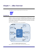
Chapter 1 – sBus Overview In this chapter, you will learn the following about the sBus serial bus: Introduction Operation Features Introduction The sBus is a serial bus on the Achronix AC22IHD1000-F53C3 (“HD1000”) FPGA to enable designers to communicate with registers on the Ethernet, SerDes, PCIe, Interlaken, and DDR hard IPs. You can write to the IP registers to configure properties and read from the registers to verify current configuration.
Operation The sBus takes serial data from the FPGA fabric sBus control logic (“Fabric”) and transmits it over a 2-bit data bus to the hard IP sBus interface for writes. For reads, the sBus takes 2-bit serial data from the hard IP to the Fabric. During a write operation, the Fabric converts the parallel data, 8-, 16-, or 32-bit wide and serializes it. The Fabric presents the address of the register to be written to and the data to the IP interface over the 2-bit serial bus.
Chapter 2 – sBus Functional Description In this chapter, you will learn the following about the sBus serial bus: Port List Read Operation Write Operation Port List The sBus interface or port uses eight signals for operation. Table 1 lists these signals and their functions. These signals can be driven directly by a state machine in the FPGA fabric. You can find more information about designs based on these topologies in Chapter_3 detailing the Master and Slave interface sections.
6. Assert the o_sbus_ack signal, when data is ready. 7. Transmit the serial data on the o_sbus_data[1:0] signals using the ordering [D1:D0]… [D31:D30] in 16 cycles. 8. De-assert the o_sbus_ack signal after 16 cycles, when the transmission is complete. Figure 3 shows the timing diagram for a 32-bit data width, sBus read operation. Figure 3: 32-bit Data Width sBus Read Operation 8-bit Data-width Mode For an 8-bit data-width mode read operation, you must do the following. 1.
Write Operation 32-bit Data-width Mode For a 32-bit data-width mode write operation, you must do the following. 1. Assert the i_sbus_req signal for 25 cycles. 2. Assert i_sbus_data[0] during the first cycle. 3. Send the LSB of the 17-bit long write address on i_sbus_data[1] during the first cycle. 4. Send the remaining 16 bits of the read address on i_sbus_data[1:0] in the following order [A2:A1]…[A16:A15] over the next 8 cycles. 5.
Figure 6: 8-bit Data Width sBus Write Operation 14 UG047, October 24, 2013
Chapter 3 – sBus Interfaces In this chapter, you will learn the following about the sBus serial bus: Master Interface Slave Interface Master Interface You have the flexibility to design the sBus master depending on your needs. You could, for example, do the following.
o_sbus_data [1:0] i_sbus_data [1:0] o_sbus_ack i_sbus_req sBus Port Control Logic Slave 1 sbus_clk reset_sbus_clk Slave 2 Fabric Figure 8: Single Master for two sBus Slaves Note: Achronix provides design examples for some of these implementations. Contact Achronix for more information and help with your specific needs. Slave Interface o_sbus_data[1:0] i_sbus_data[1:0] o_sbus_ack i_sbus_req sbus_clk sBus Port Registers The sBus slave interface typically has an 8-pin port as shown in Figure 9.
Chapter 4 – sBus Master Implementation In this chapter, you will learn the following about the sBus serial bus: Single Master for Single Slave Implementation Single Master for Multiple Slaves Implementation Multiple Masters for a Single/Multiple Slave(s) Implementation The sBus design consists primarily of defining and implementing the master control block in the HD1000 FPGA fabric.
3. Monitor the o_sbus_ack signal from the PLL sBus slave signaling the end of the write request. Note: You can simplify your design to send a fixed data pattern for the upper 24-bits. 4. Inform the user on the fabric side of the completion of the write request. Single Master for Multiple Slaves Implementation You can use a single sBus master to communicate with multiple sBus slaves on a hardened IP such as the Ethernet MAC and SerDes on the HD1000.
before a specific action, you must also consider latencies in the design to ensure that the delay from the slowest sBus link is acceptable for the application.
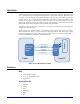
Chapter 5 – sBus Design Examples In this chapter, you will learn the following about the sBus serial bus: sBus Master Design sBus Master Operation Clocking Considerations sBus Master Design You will design and implement the sBus master in the HD1000 fabric. Figure 10 shows a typical block diagram of a master implementation showing the interface to the parallel data side (requester) and the sBus port (slave or hard IP) side.
Signal Direction o_sbus_data[1:0] Output i_sbus_ack Input o_reg_rdwr_valid Output o_reg_rd_data[Pbus_Data_Width-1:0] i_reg_wr_data[Pbus_Data_Width-1:0] i_sw_rst Output Input Input i_reg_address[16:0] i_reg_write Input Input i_reg_rw_req Input Description interface (from slave) Output serial data of sBus interface (to slave) Acknowledgement signal for read and write operation complete on sBus interface Read write operation complete indication for parallel interface Parallel Read data Parallel W
sBus Master Operation The sBus master will move from the ST_SBUS_IDLE to the ST_SBUS_ADDR state when you assert the i_sbus_req signal. Depending on whether the request is for a write or a read, as determined by the state of the i_sbus_data[0] signal, the state machine will transition to the ST_BUS_WR_DATA or ST_BUS_RD_DATA and after the completion of the cycle transition back to the ST_BUS_IDLE state. Clocking Considerations Most sBus channels must be operated at under 50 MHz clock speeds.
Appendix A – sBus Master Verilog Code // // Module Name : sbus_master_if // // Description : SBUS master module to transfer parallel register data in // serial mode to reduce the number of status ports.
parameter parameter parameter parameter ST_SBUS_ADDR ST_SBUS_WR_DATA ST_SBUS_WR ST_SBUS_RD_DATA = = = = 5'b00010; 5'b00100; 5'b01000; 5'b10000; ///////////////////////////////////////////////// always @(posedge i_clk or negedge i_rst_n) begin if (!i_rst_n) begin req_dly <= 1'b0; req_dly2 <= 1'b0; write_data <= {PBUS_DATA_WIDTH{1'b0}}; rw_address <= 'b0; is_write <= 1'b0; sbus_req_dly <= 1'b0; end else begin req_dly <= i_reg_rw_req; req_dly2 <= req_dly; sbus_req_dly <= sbus_req; if (i_reg_rw_req && ~req_
sbus_cs <= ST_SBUS_WR_DATA; end ST_SBUS_WR : begin if (i_sbus_ack) sbus_cs <= ST_SBUS_IDLE; else sbus_cs <= ST_SBUS_WR; end ST_SBUS_RD_DATA :begin if (&rdwr_data_cnt) sbus_cs <= ST_SBUS_IDLE; else sbus_cs <= ST_SBUS_RD_DATA; end default : begin sbus_cs <= ST_SBUS_IDLE; end endcase end end //////////////////////////////////////////////////////////////// // Address shift counter //////////////////////////////////////////////////////////////// always @(posedge i_clk or negedge i_rst_n) begin if (!i_rst_n) ad
if ((sbus_cs[3] && i_sbus_ack) || (sbus_cs[4] && (&rdwr_data_cnt))) o_reg_rdwr_valid <= 1'b1; else o_reg_rdwr_valid <= 1'b0; end //////////////////////////////////////////////////////////////// // RD/WR DATA shift counter //////////////////////////////////////////////////////////////// always @(posedge i_clk or negedge i_rst_n) begin if (!i_rst_n) rdwr_data_cnt <= 'b0; else begin if (sbus_cs[2] || (sbus_cs[4] && i_sbus_ack)) rdwr_data_cnt <= rdwr_data_cnt + 1; else rdwr_data_cnt <= 'b0; end end ////////////
Appendix B – Revision History The following table lists the revision history of this document. UG047, October 24, 2013 Date Version 10/24/2013 1.0 Revisions Initial Achronix release.