Speedster22i Configuration User Guide UG033 – December 18, 2013 UG033, December 18, 2013 1
Copyright Info Copyright © 2013 Achronix Semiconductor Corporation. All rights reserved. Achronix is a trademark and Speedster is a registered trademark of Achronix Semiconductor Corporation. All other trademarks are the property of their prospective owners. All specifications subject to change without notice. NOTICE of DISCLAIMER: The information given in this document is believed to be accurate and reliable.
Table of Contents Copyright Info .................................................................................................... 2 Table of Contents .............................................................................................. 3 Overview ............................................................................................................ 4 Power-Up and Configuration Sequence .......................................................... 5 Device Power-Up ............................
Overview The configuration architecture in Speedster22i HD devices is composed of a few key pieces: 1. Configuration pins enabling data transfer from an external interface to the FPGA 2. FPGA Configuration Unit (FCU) which is the IP block containing the modes, interfaces, state machines and other control logic to take data from the pins, perform the necessary FPGA mode transitions and assemble the incoming data stream into a form to be ultimately provided to the rest of the FPGA 3.
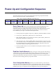
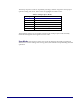
Power-Up and Configuration Sequence The requirements for the power-up and configuration sequencing for Speedster22i HD devices are illustrated in Table 1 and detailed below.
powering up VDDL. Otherwise, with SRAM cells powering up in unknown states, the presence of one-hot muxes in the routing interconnect will undoubtedly mean that there will be shorts leading to contention, and as a result unexpected behavior as far as current profiles and draws. This step can be bypassed as a debug or optimization step by asserting the BYPASS_CLR_MEM pin/signal. This is really only acceptable/feasible if the application involves re-configuring the FPGA without a power-down.
The startup sequence consists of sequentially asserting a number of signals to ensure proper operation during user mode. These events are highlighted in Table 2 below.
Configuration Modes and Pins Speedster22iHD devices have four configuration modes: CPU, Serial Flash x1, Serial Flash x4 and JTAG. The selection between the first 3 is done by tying CONFIG_MODESEL pins to the values shown in Table 3. The fourth configuration mode, which is JTAG, is independent of the mode pins and can be enabled by setting the appropriate bits in the User Data Register of the JTAG TAP Controller. Once JTAG mode is enabled, it overrides all other configuration modes until disabled.
CPU In CPU mode, an external CPU acts as the master and controls the programming operations for the FPGA. CPU mode is an 8-bit parallel interface, clocked using CPU_CLK, with chip select support to indicate valid data. This is generally the fastest programming mode as it provides for the widest data width interface and a maximum supported clock rate of 25MHz. Figure 3 below provides a block diagram of how the external CPU would be hooked up to Speedster22iHD FPGA.
In Figure 4 above: 1. After CONFIG_RSTN is deasserted, CPU_CLK needs to continue being clocked to ensure that the FPGA cycles through the FCU states and the configuration memory is cleared. At that point, CONFIG_STATUS is released and is pulled high. 2. Some time after CONFIG_STATUS is pulled high, CSN should be pulled low to begin writing the bitstream data into the FPGA. When the last set of data is written into the FPGA, CSN is pulled high. 3.
SPI Flash SCLK HOLDN DI CSN DO Speedster22iHD FPGA SCK HOLDN SDI CSN[0] SDO[0] Figure 6: Flash Connectivity to Speedster22iHD FPGA in x1 Mode This interface contains a configuration mode fast read engine that reads the data from the flash from address 0. The number of words read in the bitstream can be controlled by the bitstream by programming one of the configuration registers. This block also contains a master controller that interfaces to the JTAG unit for programming of the serial flash.
SPI Flash SCLK HOLDN DI CSN DO Speedster22iHD FPGA SCK HOLDN SDI CSN[0] SDO[0] SPI Flash SCLK HOLDN DI CSN DO CSN[1] SDO[1] SPI Flash SCLK HOLDN DI CSN DO CSN[2] SDO[2] SPI Flash SCLK HOLDN DI CSN DO CSN[3] SDO[3] Figure 7: Flash Connectivity to Speedster22iHD FPGA in x4 Mode When writing to the 4 Flash memories, the FPGA would pull the CSN for a single Flash memory in turn, write the data and then move onto the next Flash memory by pulling the corresponding CSN low.
JTAG JTAG configuration and operation mode is independent of CONFIG_MODESEL settings, although the recommendation is to ensure that the CONFIG_MODESEL values are one of '100', '001', '010' or '000' to avoid unknown or illegal states. The JTAG Tap controller design is compliant to the IEEE Std 1149.1. The TMS and TCK inputs determine whether an instruction register scan or data register scan is performed. TMS and TDI are sampled on the rising edge of TCK, while TDO changes on the falling edge.
Configuration Pins and Clock Selection Table 4 below lists the names and functions of all of the configuration and JTAG pins used in the four different configuration modes.
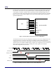
CPU_CLK TCK 1 FCU_CLK 1 0 1 0 SYSCLK 0 CONFIG_SYSCLK_BYPASS CONFIG_MODESEL[2] CONFIG_MODESEL[1] CONFIG_MODESEL[0] 3'b100 CONFIG_CLKSEL JTAG_CLKSEL (From Internal FCU) Figure 10: FPGA Configuration Clock Selection Logic Note that if programming will be done exclusively using JTAG mode, it is important to understand how to control the CONFIG_MODESEL and clock selection pins.
Bitstream File Generation Through ACE ACE has a straightforward interface to generate the bitstream files required to implement all of the supported configuration modes. The bitstream files will get generated in the ‘FPGA Programming – Generate Bitstream’ step of the compilation flow. The STAPL jam file needed for JTAG mode configuration will by default, always be generated.
UG033, December 18, 2013 3. 4x Flash: A 4x Flash (.flash4x_0-3) binary file supporting configuration from 4 flash memory devices. This the same full flash memory binary as above, but split into 4 files intended for a x4 flash memory configuration. There are NO newline characters in the files and is again completely binary. 4. CPU Mode: File formatted for CPU mode programming (.cpu). This contains the entire bitstream organized as 9 bits per line.
Design Security Speedster22iHD devices provide design security features using a 256‐bit Advanced Encryption Standard (AES) algorithm in Cipher Block Chaining (CBC) mode. The FPGA contains a non‐volatile memory (known as a high-security or HS eFuse) for the storage of the required AES key. Design security on Speedster22iHD devices is provided by putting the device in secure mode.
3. Lower VCCFHV_EFUSE[3:1], VCCRAM_EFUSE[3:1] and VDDA_NOM_E/W all back down to 1.0V. Run phase 3 steps to validate the eFuse blowing process and return the FCU back to a state to resume programming operations. Once the eFuses are blown, the Speedster22iHD FPGA will be ready to accept encrypted bitstreams as part of regular programming operation.
Revision History The following table shows the revision history for this document. 20 Date Version 12/18/2013 1.0 Revisions Initial Achronix release.