
User Macro Guide
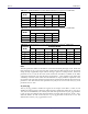
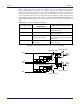
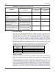
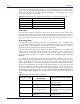
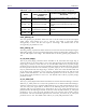
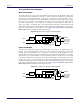
Table Of Contents
- Title - Speedster22i Macro Cell Library
- ChapterTitlePreface - Preface
- ChapterTitle - Chapter 1 – I/O Cells
- Table - Table 1-1: Supported Single-Ended Voltage Standards
- Table - Table 1-2: Supported Differential Voltage Standards
- Heading1 - IOPAD
- Heading1 - IOPAD_D
- Heading2 - Bidirectional Registered I/O Pad with Asynchronous or Synchronous Set/Reset
- Figure - Figure 1-2: IOPAD_D Logic Symbol
- Table - Table 1-7: Ports
- Table - Table 1-8: Parameters
- Table - Table 1-9: Output Function Table (txregmode = ”reg”, oeregmode = “reg”, rstmode = “async”)
- Table - Table 1-10: Output Function Table (txregmode = ”reg”, oeregmode = “reg”, rstmode = “sync”)
- Table - Table 1-11: Input Function table (rxregmode = “reg”)
- Heading3 - Verilog Instantiation Template
- Heading3 - VHDL Instantiation Template
- Heading2 - Bidirectional Registered I/O Pad with Asynchronous or Synchronous Set/Reset
- Heading1 - IOPAD_D2
- Heading2 - Bidirectional DDR I/O Pad with Asynchronous or Synchronous Set/ Reset
- Figure - Figure 1-3: IOPAD_D2 Logic Symbol
- Table - Table 1-12: Ports
- Table - Table 1-13: Parameters
- Figure - Figure 1-4: IOPAD_D2 Output Timing Diagram (assumes txdata_en = 1’b1)
- Figure - Figure 1-5: IOPAD_D2 Input Timing Diagram (assumes rxdata_en = 1’b1)
- Heading3 - Verilog Instantiation Template
- Heading3 - VHDL Instantiation Template
- Heading2 - Bidirectional DDR I/O Pad with Asynchronous or Synchronous Set/ Reset
- Heading1 - IPAD
- Heading1 - IPAD_D
- Heading1 - IPAD_D2
- Heading1 - IPAD_DIFF
- Heading1 - IPAD_DIFFD
- Heading1 - IPAD_DIFFD2
- Heading1 - OPAD
- Heading1 - OPAD_D
- Heading1 - OPAD_D2
- Heading1 - OPAD_DIFF
- Heading1 - OPAD_DIFFD
- Heading2 - Registered Differential Output Pad with Asynchronous or Synchronous Set/Reset
- Figure - Figure 1-19: OPAD_DIFFD Logic Symbol
- Table - Table 1-42: Ports
- Table - Table 1-43: Parameters
- Table - Table 1-44: Output Function Table (rstmode = “async”)
- Table - Table 1-45: Output Function Table (rstmode = “sync”)
- Heading3 - Verilog Instantiation Template
- Heading3 - VHDL Instantiation Template
- Heading2 - Registered Differential Output Pad with Asynchronous or Synchronous Set/Reset
- Heading1 - OPAD_DIFFD2
- Heading1 - TPAD
- Heading1 - TPAD_D
- ChapterTitle - Chapter 2 – Registers
- Heading1 - Naming Convention
- Heading1 - DFF
- Heading1 - DFFE
- Heading1 - DFFEC
- Heading1 - DFFEP
- Heading1 - DFFER
- Heading1 - DFFES
- Heading1 - DFFN
- Heading1 - DFFNEC
- Heading1 - DFFNEP
- Heading1 - DFFNER
- Heading1 - DFFNES
- Heading1 - DFFNR
- Heading1 - DFFNS
- Heading1 - DFFR
- Heading1 - DFFS
- ChapterTitle - Chapter 3 – Logic Functions
- ChapterTitle - Chapter 4 – Lookup Table (LUT) Functions
- ChapterTitle - Chapter 5 – Arithmetic Functions
- ChapterTitle - Chapter 6 – Memories
- Heading1 - BRAM80K
- Heading2 - 80k-bit Dual-Port Memory
- Heading2 - BRAM80K Pins
- Heading2 - Parameters
- Table - Table 6-2: BRAM80K Parameters
- Heading3 - porta_read_width(portb_read_width)
- Heading3 - porta_write_width(portb_write_width)
- Heading3 - porta_write_mode(portb_write_mode)
- Heading3 - porta_clock_polarity(portb_clock_polarity)
- Heading3 - porta_peval(portb_peval)
- Heading3 - porta_latch_rstval(portb_latch_rstval)
- Heading3 - porta_en_out_reg(portb_en_out_reg)
- Heading3 - porta_reg_rstval(portb_reg_rstval)
- Heading3 - porta_regce_priority(portb_regce_priority)
- Heading3 - porta_initval(portb_initval)
- Table - Table 6-3: Relationship of porta_initval(portb_initval) bit positions to douta,doutpa,doutpxa (doutb,doutpb,doutpxb)
- Heading3 - porta_srval(portb_srval)
- Table - Table 6-4: Relationship of porta_srval(portb_srval) bit positions to douta,doutpa,doutpxa (doutb,doutpb,doutpxb)
- Heading3 - mem_init_file
- Heading3 - initd_000 – initd_255
- Heading3 - initp_00 – initp_31
- Heading3 - initpx_00 – initpx_31
- Heading2 - Memory Organization and Data Input / Output Pin Assignments
- Table - Table 6-5: Valid Port A Width Versus Port B Width Combinations per port for n x 5 width modes
- Table - Table 6-6: Valid Port A Width Versus Port B Width Combinations per port for n x 9 width modes
- Table - Table 6-7: Valid Port A Width Versus Write Port B Combinations per port for n x 2 width modes
- Table - Table 6-8: dina(dinb) bit assignments per porta_write_width(portb_write_width) values
- Table - Table 6-9: Write Enable to Data Input Bus Mapping per Write Port Width
- Table - Table 6-10: douta(doutb) bit assignments per porta_read_width(portb_read_width) values
- Table - Table 6-11: BRAM80K Address Bus Mapping (Per Port)
- Table - Table 6-12: Mapping of Word Sizes to the Native 2048x40 Memory Locations
- Heading2 - Read and Write Operations
- Heading3 - Read Operation
- Heading3 - Write Operation
- Table - Table 6-13: BRAM Output Function Table for Latched Mode (Assumes active-high clock, port enable, and latch reset value)
- Table - Table 6-14: BRAM Output Function Table for Registered Mode (Assumes active-high clock, output register clock enable, and output register reset)
- Heading3 - Simultaneous Memory Operations
- Heading3 - Timing Diagrams
- Figure - Figure 6-3: Write-First, Latched Mode Timing Diagram
- Figure - Figure 6-4: Write-First, Registered Mode Timing Diagram
- Figure - Figure 6-5: No-Change, Latched Mode Timing Diagram
- Figure - Figure 6-6: No-Change, Registered Mode Timing Diagram
- Heading3 - Support for Read-First (Read-Before-Write) Memory Operations
- Heading2 - Memory Initialization
- Heading2 - BRAM80K Verilog Instantiation Template
- Heading2 - BRAM80K VHDL Instantiation Template
- Heading1 - BRAM80KFIFO
- Heading2 - 80k-bit FIFO Memory
- Heading2 - Parameters
- Table - Table 6-16: BRAM80KFIFO Parameters
- Heading3 - sync_mode
- Heading3 - write_width
- Table - Table 6-17: FIFO write_width versus Maximum Write Depth
- Table - Table 6-18: din, dinp, dinpx bit assignments per write_width values
- Heading3 - read_width
- Table - Table 6-19: FIFO read_width versus Maximum Read Depth
- Table - Table 6-20: dout bit assignments per read_width values
- Table - Table 6-21: Valid Read Width Versus Write Width Combinations per port for n x 5 width modes
- Table - Table 6-22: Valid Read Width Versus Write Width Combinations per port for n x 9 width modes
- Table - Table 6-23: Valid Read Width Versus Write Width Combinations per port for 2n width modes
- Heading3 - fwft
- Heading3 - en_out_reg
- Heading3 - reg_initval
- Table - Table 6-24: Relationship of reg_initval bit positions to dout,doutp,doutpx
- Heading3 - reg_srval
- Table - Table 6-25: Relationship of reg_srval bit positions to dout,doutp,doutpx
- Heading3 - reg_rstval
- Heading3 - wrrst_rstval
- Heading3 - wrrst_input_mode
- Table - Table 6-26: wrrst_input_mode Parameter Mapping.
- Figure - Figure 6-9: Read and Write Pointer Reset Input Selection Block Diagram
- Table - Table 6-27: Reset Usage Model for wrrst and rdrst Inputs
- Heading3 - wrrst_sync_stages
- Table - Table 6-28: Mapping wrrst_sync_stages Parameter Settings to Synchronization Stage Depth
- Heading3 - wrptr_sync_stages
- Table - Table 6-29: Mapping wrptr_sync_stages Parameter Settings to Synchronization Stage Depth
- Heading3 - rdrst_rstval
- Heading3 - rdrst_input_mode
- Table - Table 6-30: rdrst_input_mode Parameter Mapping.
- Heading3 - rdrst_sync_stages
- Table - Table 6-31: Mapping rdrst_sync_stages Parameter Settings to Synchronization Stage Depth
- Heading3 - rdptr_sync_stages
- Table - Table 6-32: Mapping rdptr_sync_stages Parameter Settings to Synchronization Stage Depth
- Heading3 - wrcount_sync_mode
- Heading3 - rdcount_sync_mode
- Heading3 - afull_offset
- Table - Table 6-33: Condition to Assert almost_full Flag based on afull_offset Parameter Assignment
- Heading3 - aempty_offset
- Table - Table 6-34: Condition to Assert almost_empty Flag based on afull_offset Parameter Assignment
- Heading3 - wren_polarity_sel
- Heading3 - rden_polarity_sel
- Heading3 - en_rd_when_empty
- Heading3 - en_wr_when_full
- Heading2 - Read and Write Count Outputs
- Heading2 - Status Flags
- Heading2 - Flag Latency
- Table - Table 6-35: FIFO Pointers and Status Flag Clock Domain Assignments
- Table - Table 6-36: Pointers Used for FIFO Flag Calculations
- Table - Table 6-37: Empty and Almost Empty Flag Latency in Terms of Read Clock Cycles
- Table - Table 6-38: Full and Almost Full Flag Latency in Terms of Write Clock Cycles
- Heading2 - Optional Output Register
- Heading2 - FIFO Operational Modes
- Heading2 - FIFO Operations
- Heading3 - Basic Mode FIFO Reset Operation
- Table - Table 6-40: Parameter Settings Required for Basic Mode FIFO Reset Operation
- Figure - Figure 6-12: Basic Mode FIFO Reset Timing Diagram
- Heading3 - Advanced Mode FIFO Reset Operation
- Figure - Figure 6-13: Reset Behavior Timing Diagram (Requires sync wrrst )
- Heading3 - Writing an Empty Asynchronous FIFO (sync_mode = 1’b0)
- Figure - Figure 6-14: Writing an Empty Asynchronous FIFO (sync_mode = 1’b0)
- Heading3 - Writing an Empty Synchronous FIFO (sync_mode = 1’b1)
- Figure - Figure 6-15: Writing an Empty Synchronous FIFO (sync_mode = 1’b1)
- Heading3 - Writing to an Almost Full FIFO (en_wr_when_full = 1’b0)
- Figure - Figure 6-16: Writing to an Almost Full FIFO (en_wr_when_full = 1’b0)
- Heading3 - Writing to an Almost Full FIFO (en_wr_when_full = 1’b1)
- Figure - Figure 6-17: Writing to an Almost Full FIFO (en_wr_when_full = 1’b1)
- Heading3 - Reading from an Almost Empty FIFO (en_rd_when_empty = 1’b0, fwft = 1’b0)
- Figure - Figure 6-18: Reading From an Almost Empty FIFO (en_rd_when_empty = 1’b0, fwft = 1’b0)
- Heading3 - Reading from an Almost Empty FIFO (en_rd_when_empty = 1’b0, fwft = 1’b1)
- Figure - Figure 6-19: Reading From an Almost Empty FIFO (en_rd_when_empty = 1’b0, fwft = 1’b1)
- Heading3 - Reading from an Almost Empty FIFO (en_rd_when_empty = 1’b1)
- Figure - Figure 6-20: Reading From an Almost Empty FIFO (en_rd_when_empty = 1’b1)
- Figure - Figure 6-21: Writing and Reading a Mixed-Width FIFO
- Heading3 - Limitations of Concurrent Read/Write Operations
- Heading1 - BRAM80KECC
- Heading2 - 80k-bit Simple Dual-Port Memory with Error Correction
- Heading2 - BRAM80KECC Pins
- Heading2 - Parameters
- Table - Table 6-42: BRAM80KECC Parameters
- Heading3 - en_out_reg
- Heading3 - reg_initval
- Table - Table 6-43: Relationship of reg_initval bit positions to dout,doutp,doutpx
- Heading3 - reg_srval
- Table - Table 6-44: Relationship of reg_srval bit positions to dout,doutp,doutpx
- Heading3 - reg_rstval
- Heading3 - encoder_enable
- Heading3 - decoder_enable
- Heading3 - mem_init_file
- Heading3 - initd_000 – initd_255
- Heading3 - initp_0 – initp_31
- Heading3 - initpx_0 – initpx_31
- Heading2 - BRAM80KECC Modes of Operation
- Heading2 - ECC Encode/Decode Operation Mode
- Heading2 - ECC Encode-Only Operation Mode
- Heading2 - ECC Decode-Only Operation Mode
- Heading1 - BRAM80KECCFIFO
- Heading1 - LRAM640
- Heading1 - LRAMFIFO
- Heading2 - LRAM-Based 64-Word FIFO Memory
- Heading2 - Parameters
- Table - Table 6-51: LRAMFIFO Parameters
- Heading3 - width
- Heading3 - depth
- Heading3 - ptr_sync_mode
- Heading3 - wrptr_sync_stages
- Table - Table 6-52: Mapping wrptr_sync_stages Parameter Settings to Synchronization Stage Depth
- Figure - Figure 6-33: Write Pointer Synchronizer Block Diagram
- Heading3 - rdptr_sync_stages
- Table - Table 6-53: Mapping rdptr_sync_stages Parameter Settings to Synchronization Stage Depth
- Figure - Figure 6-34: Read Pointer Synchronizer Block Diagram
- Heading3 - rst_sync_mode
- Heading3 - wrrst_sync_stages
- Table - Table 6-54: Mapping wrrst_sync_stages Parameter Settings to Synchronization Stage Depth
- Figure - Figure 6-35: Write Pointer Reset Input Selection Block Diagram
- Heading3 - rdrst_sync_stages
- Table - Table 6-55: Mapping rdrst_sync_stages Parameter Settings to Synchronization Stage Depth
- Figure - Figure 6-36: Read Pointer Reset Input Selection Block Diagram
- Heading3 - afull_offset
- Table - Table 6-56: Condition to Assert almost_full Flag based on afull_offset Parameter Assignment
- Heading3 - aempty_offset
- Table - Table 6-57: Condition to Assert almost_empty Flag based on aempty_offset Parameter Assignment
- Heading2 - Status Flags
- Heading2 - Flag Latency in Asynchronous Mode (ptr_sync_mode = 1’b0)
- Table - Table 6-58: FIFO Pointers and Status Flag Clock Domain Assignments
- Table - Table 6-59: Pointers Used for FIFO Flag Calculations (ptr_sync_mode = 1’b0)
- Table - Table 6-60: Empty and Almost Empty Flag Latency in Terms of Read Clock Cycles(ptr_sync_mode =1’b0)
- Table - Table 6-61: Full and Almost Full Flag Latency in Terms of Write Clock Cycles(ptr_sync_mode = 1’b0)
- Heading2 - Flag Latency in Synchronous Mode (ptr_sync_mode = 1’b1)
- Heading2 - FIFO Operational Modes
- Heading2 - FIFO Operations
- Heading3 - Asynchronous FIFO Mode Reset Operation
- Figure - Figure 6-37: Asynchronous FIFO Mode Reset Timing Diagram
- Heading3 - Writing an Empty Asynchronous FIFO (ptr_sync_mode = 1’b0)
- Figure - Figure 6-38: Writing an Empty Asynchronous FIFO (ptr_sync_mode = 1’b0)
- Heading3 - Writing an Empty Synchronous FIFO (ptr_sync_mode = 1’b1)
- Figure - Figure 6-39: Writing an Empty Synchronous FIFO (ptr_sync_mode = 1’b1)
- Heading3 - Writing to an Almost Full FIFO
- Figure - Figure 6-40: Writing to an Almost Full FIFO
- Heading3 - Reading from an Almost Empty FIFO
- Figure - Figure 6-41: Reading From an Almost Empty FIFO
- Heading1 - BRAM80K
- ChapterTitle - Chapter 7 – Multipliers
- Heading1 - BMACC56
- Heading2 - 28 x 28 Multiplier / Accumulator
- Heading2 - BMACC56 Pins
- Heading2 - Parameters
- Table - Table 7-3: BMACC56 Parameters
- Heading3 - init_a
- Heading3 - init_b
- Heading3 - init_sub
- Heading3 - init_cin
- Heading3 - init_mask_adda
- Heading3 - init_dout
- Heading3 - init_cout
- Heading3 - rst_value_a
- Heading3 - rst_value_b
- Heading3 - rst_value_sub
- Heading3 - rst_value_cin
- Heading3 - rst_value_mask_adda
- Heading3 - rst_value_dout
- Heading3 - rst_value_cout
- Heading3 - regce_priority_a
- Heading3 - regce_priority_b
- Heading3 - regce_priority_sub
- Heading3 - regce_priority_cin
- Heading3 - regce_priority_dout
- Heading3 - reg_a
- Heading3 - reg_b
- Heading3 - reg_addb
- Heading3 - reg_mask_adda
- Heading3 - reg_dout
- Heading3 - reg_cout
- Heading3 - sel_cascade_in
- Heading3 - sel_cascade_out
- Heading3 - sel_cin
- Table - Table 7-4: Add/Sub Block Carry Input Assignment
- Heading3 - sel_sub
- Table - Table 7-5: Add/Sub Block Sub Input Assignment
- Heading3 - mult_bypass
- Heading3 - clock_edge
- Heading2 - BMACC56 Verilog Instantiation Template
- Heading2 - BMACC56 VHDL Instantiation Template
- Heading1 - BMULT28X28
- Heading1 - BMACC56
- ChapterTitle - Chapter 8 – Special Functions
- ChapterTitle - Chapter 9 – PLL/DLL Clock Generators
- Heading1 - ACX_CLKGEN
- Heading2 - Phase-Locked Loop Clock Generator
- Heading2 - ACX_CLKGEN Pins
- Heading2 - Parameters
- Heading2 - ACX_CLKGEN Components
- Heading3 - Reference Divider
- Heading3 - Voltage Controlled Oscillator (VCO)
- Heading3 - Phase Rotator with Output Divider
- Heading3 - Output Synthesizer
- Heading3 - Phase Frequency Detector (PFD)
- Heading3 - Feedback Divider
- Heading3 - Clock Feedback Selection
- Table - Table 9-3: Clock Feedback Selection
- Heading3 - PLL Control
- Heading3 - Serial Control Bus (SCB)
- Figure - Figure 9-3: Serial Control Bus Read Operation
- Figure - Figure 9-4: Serial Control Bus Write Operation
- Heading2 - Control Status Registers (CSR) Register Description
- Heading1 - ACX_CLKGEN
- ChapterTitlePreface - Revision History

Memories BRAM80KFIFO
Speedster22i Macro Cell Library
AchronixSemiconductorProprietary PAGE 128
Table 6-27: Reset Usage Model for wrrst and rdrst Inputs
Use Model
Required wrrst and rdrst
c
onnections
Required
wrrst_input_mode
assignme
nt
Required
rdrst_input_mode
assignment
A single reset in the rdclk domain
resets both the read and write
pointers.
The user reset is connected to the
rdrst input. The wrrst signal is tied
inactive.
2’b11 2’b00
A single reset in the wrclk domain
r
esets both the read and write
pointers.
The user reset is connected to the
wrrst input. The rdrst signal is tied
inactive.
2’b00 2’b11
A single asychronous reset resets
both the
read and write pointers.
The user reset is connected to
both the wrrst and rdrst inputs.
2’b11 2’b11
The wrrst reset in the wrclk
domain or the r
drst reset in the
rdclk domain resets both the read
and write pointers.
The user reset in the wrclk domain
i
s connected to the wrrst input.
The user reset in the rdclk domain
is connected to the rdrst input.
2’b10 2’b10
The wrrst reset in the wrclk
domain r
esets the write pointer.
The rdrst reset in the rdclk domain
resets the read pointer.
The user reset in the wrclk domain
i
s connected to the wrrst input.
The user reset in the rdclk domain
is connected to the rdrst input.
2’b00 2’b00
wrrst_sync_stages
The wrrst_sync_stages parameter defines the number of stages of registers used to
synchronize the wrrst input pin to the rdclk clock domain if the wrrst signal is usedbythe
Read Pointer Reset. The value of the wrrst_sync_stages parameter is only used if the
rdrst_input_modeissetto2’b10or2’b11.Themappingofthewrrst_sync_stagesparameter
va
lue to the number of sychronization stages is defined in Table 6‐28
: Mapping
wrrst_sync_stages Parameter Sett
ings to Synchronization Stage Depth, where each stage
corresponds to a re
gister in the Write Reset Synchronizer shown in Figure 6‐9: Read and
WritePo
interResetInputSelectionBlockDiagram.Forexample,settingwrrst_sync_stages
to2’
b00configuresthewrrstsynchronizationcircuittohavetwoback‐to‐backregistersinthe
WriteResetSynchonizer.Thedefaultvalueofthewrrst_sync_stagesparameteris2’b00.
Table 6-28: Mapping wrrst_sync_stages Parameter Settings to S
ynchronization Stage Depth
wrrst_sync_stages Write Reset Synchronization Stage Depth
2’b00 2
2’b01 3
2’b10 4
2’b11 5
wrptr_sync_stages
The wrptr_sync_stages parameter defines the number of stages used in the Write Pointer
SynchonizercircuitthatsynchronizestheWritePointertotherdclkclockdomain.Whenthe
FIFO is in asynchronous mode, (sync_mode = 1’b0), the output of the synchonized Write
Pointeriscomparedtothe ReadPointertogeneratetheemptyandalmost_emptyfl
ags.The
synchronizedWritePointermayalsoberoutedtothewrcounteroutput(wrcount_sync_mode
= 1’b0). The mapping of the wrptr_sync_stages parameter value to the number of sychro ‐
nizationstagesisde
finedinTable6‐29: Mappingwrptr_sync_stagesParameterSettingsto
SynchronizationStageDe
pth,whereeachstagecorrespondstoaregisterintheWritePointer
Synchronizer circuit sho
wn in Figure 6‐10: Write Pointer Synchronizer Block Diagram.
Higher va
lues forthe wrptr_sync_stages parameter reduce the possibility of a metastable