
User Macro Guide
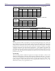
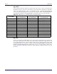
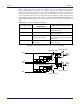
Table Of Contents
- Title - Speedster22i Macro Cell Library
- ChapterTitlePreface - Preface
- ChapterTitle - Chapter 1 – I/O Cells
- Table - Table 1-1: Supported Single-Ended Voltage Standards
- Table - Table 1-2: Supported Differential Voltage Standards
- Heading1 - IOPAD
- Heading1 - IOPAD_D
- Heading2 - Bidirectional Registered I/O Pad with Asynchronous or Synchronous Set/Reset
- Figure - Figure 1-2: IOPAD_D Logic Symbol
- Table - Table 1-7: Ports
- Table - Table 1-8: Parameters
- Table - Table 1-9: Output Function Table (txregmode = ”reg”, oeregmode = “reg”, rstmode = “async”)
- Table - Table 1-10: Output Function Table (txregmode = ”reg”, oeregmode = “reg”, rstmode = “sync”)
- Table - Table 1-11: Input Function table (rxregmode = “reg”)
- Heading3 - Verilog Instantiation Template
- Heading3 - VHDL Instantiation Template
- Heading2 - Bidirectional Registered I/O Pad with Asynchronous or Synchronous Set/Reset
- Heading1 - IOPAD_D2
- Heading2 - Bidirectional DDR I/O Pad with Asynchronous or Synchronous Set/ Reset
- Figure - Figure 1-3: IOPAD_D2 Logic Symbol
- Table - Table 1-12: Ports
- Table - Table 1-13: Parameters
- Figure - Figure 1-4: IOPAD_D2 Output Timing Diagram (assumes txdata_en = 1’b1)
- Figure - Figure 1-5: IOPAD_D2 Input Timing Diagram (assumes rxdata_en = 1’b1)
- Heading3 - Verilog Instantiation Template
- Heading3 - VHDL Instantiation Template
- Heading2 - Bidirectional DDR I/O Pad with Asynchronous or Synchronous Set/ Reset
- Heading1 - IPAD
- Heading1 - IPAD_D
- Heading1 - IPAD_D2
- Heading1 - IPAD_DIFF
- Heading1 - IPAD_DIFFD
- Heading1 - IPAD_DIFFD2
- Heading1 - OPAD
- Heading1 - OPAD_D
- Heading1 - OPAD_D2
- Heading1 - OPAD_DIFF
- Heading1 - OPAD_DIFFD
- Heading2 - Registered Differential Output Pad with Asynchronous or Synchronous Set/Reset
- Figure - Figure 1-19: OPAD_DIFFD Logic Symbol
- Table - Table 1-42: Ports
- Table - Table 1-43: Parameters
- Table - Table 1-44: Output Function Table (rstmode = “async”)
- Table - Table 1-45: Output Function Table (rstmode = “sync”)
- Heading3 - Verilog Instantiation Template
- Heading3 - VHDL Instantiation Template
- Heading2 - Registered Differential Output Pad with Asynchronous or Synchronous Set/Reset
- Heading1 - OPAD_DIFFD2
- Heading1 - TPAD
- Heading1 - TPAD_D
- ChapterTitle - Chapter 2 – Registers
- Heading1 - Naming Convention
- Heading1 - DFF
- Heading1 - DFFE
- Heading1 - DFFEC
- Heading1 - DFFEP
- Heading1 - DFFER
- Heading1 - DFFES
- Heading1 - DFFN
- Heading1 - DFFNEC
- Heading1 - DFFNEP
- Heading1 - DFFNER
- Heading1 - DFFNES
- Heading1 - DFFNR
- Heading1 - DFFNS
- Heading1 - DFFR
- Heading1 - DFFS
- ChapterTitle - Chapter 3 – Logic Functions
- ChapterTitle - Chapter 4 – Lookup Table (LUT) Functions
- ChapterTitle - Chapter 5 – Arithmetic Functions
- ChapterTitle - Chapter 6 – Memories
- Heading1 - BRAM80K
- Heading2 - 80k-bit Dual-Port Memory
- Heading2 - BRAM80K Pins
- Heading2 - Parameters
- Table - Table 6-2: BRAM80K Parameters
- Heading3 - porta_read_width(portb_read_width)
- Heading3 - porta_write_width(portb_write_width)
- Heading3 - porta_write_mode(portb_write_mode)
- Heading3 - porta_clock_polarity(portb_clock_polarity)
- Heading3 - porta_peval(portb_peval)
- Heading3 - porta_latch_rstval(portb_latch_rstval)
- Heading3 - porta_en_out_reg(portb_en_out_reg)
- Heading3 - porta_reg_rstval(portb_reg_rstval)
- Heading3 - porta_regce_priority(portb_regce_priority)
- Heading3 - porta_initval(portb_initval)
- Table - Table 6-3: Relationship of porta_initval(portb_initval) bit positions to douta,doutpa,doutpxa (doutb,doutpb,doutpxb)
- Heading3 - porta_srval(portb_srval)
- Table - Table 6-4: Relationship of porta_srval(portb_srval) bit positions to douta,doutpa,doutpxa (doutb,doutpb,doutpxb)
- Heading3 - mem_init_file
- Heading3 - initd_000 – initd_255
- Heading3 - initp_00 – initp_31
- Heading3 - initpx_00 – initpx_31
- Heading2 - Memory Organization and Data Input / Output Pin Assignments
- Table - Table 6-5: Valid Port A Width Versus Port B Width Combinations per port for n x 5 width modes
- Table - Table 6-6: Valid Port A Width Versus Port B Width Combinations per port for n x 9 width modes
- Table - Table 6-7: Valid Port A Width Versus Write Port B Combinations per port for n x 2 width modes
- Table - Table 6-8: dina(dinb) bit assignments per porta_write_width(portb_write_width) values
- Table - Table 6-9: Write Enable to Data Input Bus Mapping per Write Port Width
- Table - Table 6-10: douta(doutb) bit assignments per porta_read_width(portb_read_width) values
- Table - Table 6-11: BRAM80K Address Bus Mapping (Per Port)
- Table - Table 6-12: Mapping of Word Sizes to the Native 2048x40 Memory Locations
- Heading2 - Read and Write Operations
- Heading3 - Read Operation
- Heading3 - Write Operation
- Table - Table 6-13: BRAM Output Function Table for Latched Mode (Assumes active-high clock, port enable, and latch reset value)
- Table - Table 6-14: BRAM Output Function Table for Registered Mode (Assumes active-high clock, output register clock enable, and output register reset)
- Heading3 - Simultaneous Memory Operations
- Heading3 - Timing Diagrams
- Figure - Figure 6-3: Write-First, Latched Mode Timing Diagram
- Figure - Figure 6-4: Write-First, Registered Mode Timing Diagram
- Figure - Figure 6-5: No-Change, Latched Mode Timing Diagram
- Figure - Figure 6-6: No-Change, Registered Mode Timing Diagram
- Heading3 - Support for Read-First (Read-Before-Write) Memory Operations
- Heading2 - Memory Initialization
- Heading2 - BRAM80K Verilog Instantiation Template
- Heading2 - BRAM80K VHDL Instantiation Template
- Heading1 - BRAM80KFIFO
- Heading2 - 80k-bit FIFO Memory
- Heading2 - Parameters
- Table - Table 6-16: BRAM80KFIFO Parameters
- Heading3 - sync_mode
- Heading3 - write_width
- Table - Table 6-17: FIFO write_width versus Maximum Write Depth
- Table - Table 6-18: din, dinp, dinpx bit assignments per write_width values
- Heading3 - read_width
- Table - Table 6-19: FIFO read_width versus Maximum Read Depth
- Table - Table 6-20: dout bit assignments per read_width values
- Table - Table 6-21: Valid Read Width Versus Write Width Combinations per port for n x 5 width modes
- Table - Table 6-22: Valid Read Width Versus Write Width Combinations per port for n x 9 width modes
- Table - Table 6-23: Valid Read Width Versus Write Width Combinations per port for 2n width modes
- Heading3 - fwft
- Heading3 - en_out_reg
- Heading3 - reg_initval
- Table - Table 6-24: Relationship of reg_initval bit positions to dout,doutp,doutpx
- Heading3 - reg_srval
- Table - Table 6-25: Relationship of reg_srval bit positions to dout,doutp,doutpx
- Heading3 - reg_rstval
- Heading3 - wrrst_rstval
- Heading3 - wrrst_input_mode
- Table - Table 6-26: wrrst_input_mode Parameter Mapping.
- Figure - Figure 6-9: Read and Write Pointer Reset Input Selection Block Diagram
- Table - Table 6-27: Reset Usage Model for wrrst and rdrst Inputs
- Heading3 - wrrst_sync_stages
- Table - Table 6-28: Mapping wrrst_sync_stages Parameter Settings to Synchronization Stage Depth
- Heading3 - wrptr_sync_stages
- Table - Table 6-29: Mapping wrptr_sync_stages Parameter Settings to Synchronization Stage Depth
- Heading3 - rdrst_rstval
- Heading3 - rdrst_input_mode
- Table - Table 6-30: rdrst_input_mode Parameter Mapping.
- Heading3 - rdrst_sync_stages
- Table - Table 6-31: Mapping rdrst_sync_stages Parameter Settings to Synchronization Stage Depth
- Heading3 - rdptr_sync_stages
- Table - Table 6-32: Mapping rdptr_sync_stages Parameter Settings to Synchronization Stage Depth
- Heading3 - wrcount_sync_mode
- Heading3 - rdcount_sync_mode
- Heading3 - afull_offset
- Table - Table 6-33: Condition to Assert almost_full Flag based on afull_offset Parameter Assignment
- Heading3 - aempty_offset
- Table - Table 6-34: Condition to Assert almost_empty Flag based on afull_offset Parameter Assignment
- Heading3 - wren_polarity_sel
- Heading3 - rden_polarity_sel
- Heading3 - en_rd_when_empty
- Heading3 - en_wr_when_full
- Heading2 - Read and Write Count Outputs
- Heading2 - Status Flags
- Heading2 - Flag Latency
- Table - Table 6-35: FIFO Pointers and Status Flag Clock Domain Assignments
- Table - Table 6-36: Pointers Used for FIFO Flag Calculations
- Table - Table 6-37: Empty and Almost Empty Flag Latency in Terms of Read Clock Cycles
- Table - Table 6-38: Full and Almost Full Flag Latency in Terms of Write Clock Cycles
- Heading2 - Optional Output Register
- Heading2 - FIFO Operational Modes
- Heading2 - FIFO Operations
- Heading3 - Basic Mode FIFO Reset Operation
- Table - Table 6-40: Parameter Settings Required for Basic Mode FIFO Reset Operation
- Figure - Figure 6-12: Basic Mode FIFO Reset Timing Diagram
- Heading3 - Advanced Mode FIFO Reset Operation
- Figure - Figure 6-13: Reset Behavior Timing Diagram (Requires sync wrrst )
- Heading3 - Writing an Empty Asynchronous FIFO (sync_mode = 1’b0)
- Figure - Figure 6-14: Writing an Empty Asynchronous FIFO (sync_mode = 1’b0)
- Heading3 - Writing an Empty Synchronous FIFO (sync_mode = 1’b1)
- Figure - Figure 6-15: Writing an Empty Synchronous FIFO (sync_mode = 1’b1)
- Heading3 - Writing to an Almost Full FIFO (en_wr_when_full = 1’b0)
- Figure - Figure 6-16: Writing to an Almost Full FIFO (en_wr_when_full = 1’b0)
- Heading3 - Writing to an Almost Full FIFO (en_wr_when_full = 1’b1)
- Figure - Figure 6-17: Writing to an Almost Full FIFO (en_wr_when_full = 1’b1)
- Heading3 - Reading from an Almost Empty FIFO (en_rd_when_empty = 1’b0, fwft = 1’b0)
- Figure - Figure 6-18: Reading From an Almost Empty FIFO (en_rd_when_empty = 1’b0, fwft = 1’b0)
- Heading3 - Reading from an Almost Empty FIFO (en_rd_when_empty = 1’b0, fwft = 1’b1)
- Figure - Figure 6-19: Reading From an Almost Empty FIFO (en_rd_when_empty = 1’b0, fwft = 1’b1)
- Heading3 - Reading from an Almost Empty FIFO (en_rd_when_empty = 1’b1)
- Figure - Figure 6-20: Reading From an Almost Empty FIFO (en_rd_when_empty = 1’b1)
- Figure - Figure 6-21: Writing and Reading a Mixed-Width FIFO
- Heading3 - Limitations of Concurrent Read/Write Operations
- Heading1 - BRAM80KECC
- Heading2 - 80k-bit Simple Dual-Port Memory with Error Correction
- Heading2 - BRAM80KECC Pins
- Heading2 - Parameters
- Table - Table 6-42: BRAM80KECC Parameters
- Heading3 - en_out_reg
- Heading3 - reg_initval
- Table - Table 6-43: Relationship of reg_initval bit positions to dout,doutp,doutpx
- Heading3 - reg_srval
- Table - Table 6-44: Relationship of reg_srval bit positions to dout,doutp,doutpx
- Heading3 - reg_rstval
- Heading3 - encoder_enable
- Heading3 - decoder_enable
- Heading3 - mem_init_file
- Heading3 - initd_000 – initd_255
- Heading3 - initp_0 – initp_31
- Heading3 - initpx_0 – initpx_31
- Heading2 - BRAM80KECC Modes of Operation
- Heading2 - ECC Encode/Decode Operation Mode
- Heading2 - ECC Encode-Only Operation Mode
- Heading2 - ECC Decode-Only Operation Mode
- Heading1 - BRAM80KECCFIFO
- Heading1 - LRAM640
- Heading1 - LRAMFIFO
- Heading2 - LRAM-Based 64-Word FIFO Memory
- Heading2 - Parameters
- Table - Table 6-51: LRAMFIFO Parameters
- Heading3 - width
- Heading3 - depth
- Heading3 - ptr_sync_mode
- Heading3 - wrptr_sync_stages
- Table - Table 6-52: Mapping wrptr_sync_stages Parameter Settings to Synchronization Stage Depth
- Figure - Figure 6-33: Write Pointer Synchronizer Block Diagram
- Heading3 - rdptr_sync_stages
- Table - Table 6-53: Mapping rdptr_sync_stages Parameter Settings to Synchronization Stage Depth
- Figure - Figure 6-34: Read Pointer Synchronizer Block Diagram
- Heading3 - rst_sync_mode
- Heading3 - wrrst_sync_stages
- Table - Table 6-54: Mapping wrrst_sync_stages Parameter Settings to Synchronization Stage Depth
- Figure - Figure 6-35: Write Pointer Reset Input Selection Block Diagram
- Heading3 - rdrst_sync_stages
- Table - Table 6-55: Mapping rdrst_sync_stages Parameter Settings to Synchronization Stage Depth
- Figure - Figure 6-36: Read Pointer Reset Input Selection Block Diagram
- Heading3 - afull_offset
- Table - Table 6-56: Condition to Assert almost_full Flag based on afull_offset Parameter Assignment
- Heading3 - aempty_offset
- Table - Table 6-57: Condition to Assert almost_empty Flag based on aempty_offset Parameter Assignment
- Heading2 - Status Flags
- Heading2 - Flag Latency in Asynchronous Mode (ptr_sync_mode = 1’b0)
- Table - Table 6-58: FIFO Pointers and Status Flag Clock Domain Assignments
- Table - Table 6-59: Pointers Used for FIFO Flag Calculations (ptr_sync_mode = 1’b0)
- Table - Table 6-60: Empty and Almost Empty Flag Latency in Terms of Read Clock Cycles(ptr_sync_mode =1’b0)
- Table - Table 6-61: Full and Almost Full Flag Latency in Terms of Write Clock Cycles(ptr_sync_mode = 1’b0)
- Heading2 - Flag Latency in Synchronous Mode (ptr_sync_mode = 1’b1)
- Heading2 - FIFO Operational Modes
- Heading2 - FIFO Operations
- Heading3 - Asynchronous FIFO Mode Reset Operation
- Figure - Figure 6-37: Asynchronous FIFO Mode Reset Timing Diagram
- Heading3 - Writing an Empty Asynchronous FIFO (ptr_sync_mode = 1’b0)
- Figure - Figure 6-38: Writing an Empty Asynchronous FIFO (ptr_sync_mode = 1’b0)
- Heading3 - Writing an Empty Synchronous FIFO (ptr_sync_mode = 1’b1)
- Figure - Figure 6-39: Writing an Empty Synchronous FIFO (ptr_sync_mode = 1’b1)
- Heading3 - Writing to an Almost Full FIFO
- Figure - Figure 6-40: Writing to an Almost Full FIFO
- Heading3 - Reading from an Almost Empty FIFO
- Figure - Figure 6-41: Reading From an Almost Empty FIFO
- Heading1 - BRAM80K
- ChapterTitle - Chapter 7 – Multipliers
- Heading1 - BMACC56
- Heading2 - 28 x 28 Multiplier / Accumulator
- Heading2 - BMACC56 Pins
- Heading2 - Parameters
- Table - Table 7-3: BMACC56 Parameters
- Heading3 - init_a
- Heading3 - init_b
- Heading3 - init_sub
- Heading3 - init_cin
- Heading3 - init_mask_adda
- Heading3 - init_dout
- Heading3 - init_cout
- Heading3 - rst_value_a
- Heading3 - rst_value_b
- Heading3 - rst_value_sub
- Heading3 - rst_value_cin
- Heading3 - rst_value_mask_adda
- Heading3 - rst_value_dout
- Heading3 - rst_value_cout
- Heading3 - regce_priority_a
- Heading3 - regce_priority_b
- Heading3 - regce_priority_sub
- Heading3 - regce_priority_cin
- Heading3 - regce_priority_dout
- Heading3 - reg_a
- Heading3 - reg_b
- Heading3 - reg_addb
- Heading3 - reg_mask_adda
- Heading3 - reg_dout
- Heading3 - reg_cout
- Heading3 - sel_cascade_in
- Heading3 - sel_cascade_out
- Heading3 - sel_cin
- Table - Table 7-4: Add/Sub Block Carry Input Assignment
- Heading3 - sel_sub
- Table - Table 7-5: Add/Sub Block Sub Input Assignment
- Heading3 - mult_bypass
- Heading3 - clock_edge
- Heading2 - BMACC56 Verilog Instantiation Template
- Heading2 - BMACC56 VHDL Instantiation Template
- Heading1 - BMULT28X28
- Heading1 - BMACC56
- ChapterTitle - Chapter 8 – Special Functions
- ChapterTitle - Chapter 9 – PLL/DLL Clock Generators
- Heading1 - ACX_CLKGEN
- Heading2 - Phase-Locked Loop Clock Generator
- Heading2 - ACX_CLKGEN Pins
- Heading2 - Parameters
- Heading2 - ACX_CLKGEN Components
- Heading3 - Reference Divider
- Heading3 - Voltage Controlled Oscillator (VCO)
- Heading3 - Phase Rotator with Output Divider
- Heading3 - Output Synthesizer
- Heading3 - Phase Frequency Detector (PFD)
- Heading3 - Feedback Divider
- Heading3 - Clock Feedback Selection
- Table - Table 9-3: Clock Feedback Selection
- Heading3 - PLL Control
- Heading3 - Serial Control Bus (SCB)
- Figure - Figure 9-3: Serial Control Bus Read Operation
- Figure - Figure 9-4: Serial Control Bus Write Operation
- Heading2 - Control Status Registers (CSR) Register Description
- Heading1 - ACX_CLKGEN
- ChapterTitlePreface - Revision History

Memories BRAM80KFIFO
Speedster22i Macro Cell Library
AchronixSemiconductorProprietary PAGE 129
event when transferring the Write Pointer across clock domains. As an example, setting
wrptr_sync_stagesto 2’b00 configures the write pointer synchronization circuit to have two
back‐to‐back registers in the Write Pointer Synchonizer.The default value of the
wrptr_sync_stagesparameteris2’b00.
Table 6-29: Mapping wrptr_sync_stages Parameter Settings to Synchronization Stage Depth
wrptr_sync_stages Write Pointer Synchronization Stage Depth
2’b00 2
2’b01 3
2’b10 4
2’b11 5
rdrst_rstval
The rdrst_rstval parameter defines the active level of the read port reset (rdrst ) input.
Assigningavalueof1’b0tordrst_rstvalconfiguresthereadportresetinputtohaveanactive‐
lowsynchronousreset,whileassigningavalueof1’b1configuresthereadportresetinpu tto
haveanactive‐highsynchronousreset.Thedef
aultvalueofthewrrst_rstvalparameteris1’b1.
rdrst_input_mode
The rdrst_input_mode parameter defines how the Read Pointer is reset. The FIFO macro
providestheuserwithseveraloptionstoresettheFIFOeithersychronouslyortosynchronize
the reset input to the appropriate clock domain within the FIFO without the need to
implementseparatesynchronizationcircuitryintheFPGAfabric.
The Read Po
inter Reset input of the Read Pointer must be synchronous to the rdclk clock
domain.The user must either provide a synchronous reset via the wrrst or rdrst inpu ts or
synchronize the wrrst input.The method to reset the Read Pointer is selected via the
rdrst_input_mode paramter is defined in Table 6‐30
: rdrst_input_mode Parameter
Mapping.
By configuring the wrrst_
input_mode and rdrst_input_mode parameters, the user may
choosetohavetheFIFOWritePointerandReadPointerresetbyoneorbothofthewrrst/rdrst
inputs.Alternatively, the user may also program the reset of the Write Pointer and Read
Pointer independently of each other.For example, the us
er may program the FIFO reset
inputstoactindependentlyofeachothersothattheReadPointerisresetexclusivelybythe
rdrst input to allow the contents of a previously written FIFO to be reread.Note that as a
result of the Read Pointer reset, the flag outputs are also updated. A block di
agram of the
ReadPointerResetselectioncircuitryisshowninFigure6‐9: ReadandWritePo
interReset
Input S
election Block Diagram. The default value of the rdrst_input_mode parameter is
2’b10.
Table 6-30: rdrst_input_mode Parameter Mapping.
rdrst_input_mode
Selected Input for Read
Po
inter Reset
Read Pointer Reset Use Model
2’b00 rdrst input resets Read Pointer Requires rdrst input is synchronous to
rdclk clock domain
2’b01 wrrst input resets Read Pointer Requires wrrst input is synchronous to
r
dclk clock domain
2’b10 rdrst or synchronized wrrst
input r
esets Read Pointer
Read pointer may be reset by either
the synchronous rdrst or synchonized
wrrst inputs.
2’b11 Synchronized wrrst input resets
Re
ad Pointer
Read Pointer only reset by synchro-
nized wrrst input.