
User Macro Guide
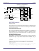
Table Of Contents
- Title - Speedster22i Macro Cell Library
- ChapterTitlePreface - Preface
- ChapterTitle - Chapter 1 – I/O Cells
- Table - Table 1-1: Supported Single-Ended Voltage Standards
- Table - Table 1-2: Supported Differential Voltage Standards
- Heading1 - IOPAD
- Heading1 - IOPAD_D
- Heading2 - Bidirectional Registered I/O Pad with Asynchronous or Synchronous Set/Reset
- Figure - Figure 1-2: IOPAD_D Logic Symbol
- Table - Table 1-7: Ports
- Table - Table 1-8: Parameters
- Table - Table 1-9: Output Function Table (txregmode = ”reg”, oeregmode = “reg”, rstmode = “async”)
- Table - Table 1-10: Output Function Table (txregmode = ”reg”, oeregmode = “reg”, rstmode = “sync”)
- Table - Table 1-11: Input Function table (rxregmode = “reg”)
- Heading3 - Verilog Instantiation Template
- Heading3 - VHDL Instantiation Template
- Heading2 - Bidirectional Registered I/O Pad with Asynchronous or Synchronous Set/Reset
- Heading1 - IOPAD_D2
- Heading2 - Bidirectional DDR I/O Pad with Asynchronous or Synchronous Set/ Reset
- Figure - Figure 1-3: IOPAD_D2 Logic Symbol
- Table - Table 1-12: Ports
- Table - Table 1-13: Parameters
- Figure - Figure 1-4: IOPAD_D2 Output Timing Diagram (assumes txdata_en = 1’b1)
- Figure - Figure 1-5: IOPAD_D2 Input Timing Diagram (assumes rxdata_en = 1’b1)
- Heading3 - Verilog Instantiation Template
- Heading3 - VHDL Instantiation Template
- Heading2 - Bidirectional DDR I/O Pad with Asynchronous or Synchronous Set/ Reset
- Heading1 - IPAD
- Heading1 - IPAD_D
- Heading1 - IPAD_D2
- Heading1 - IPAD_DIFF
- Heading1 - IPAD_DIFFD
- Heading1 - IPAD_DIFFD2
- Heading1 - OPAD
- Heading1 - OPAD_D
- Heading1 - OPAD_D2
- Heading1 - OPAD_DIFF
- Heading1 - OPAD_DIFFD
- Heading2 - Registered Differential Output Pad with Asynchronous or Synchronous Set/Reset
- Figure - Figure 1-19: OPAD_DIFFD Logic Symbol
- Table - Table 1-42: Ports
- Table - Table 1-43: Parameters
- Table - Table 1-44: Output Function Table (rstmode = “async”)
- Table - Table 1-45: Output Function Table (rstmode = “sync”)
- Heading3 - Verilog Instantiation Template
- Heading3 - VHDL Instantiation Template
- Heading2 - Registered Differential Output Pad with Asynchronous or Synchronous Set/Reset
- Heading1 - OPAD_DIFFD2
- Heading1 - TPAD
- Heading1 - TPAD_D
- ChapterTitle - Chapter 2 – Registers
- Heading1 - Naming Convention
- Heading1 - DFF
- Heading1 - DFFE
- Heading1 - DFFEC
- Heading1 - DFFEP
- Heading1 - DFFER
- Heading1 - DFFES
- Heading1 - DFFN
- Heading1 - DFFNEC
- Heading1 - DFFNEP
- Heading1 - DFFNER
- Heading1 - DFFNES
- Heading1 - DFFNR
- Heading1 - DFFNS
- Heading1 - DFFR
- Heading1 - DFFS
- ChapterTitle - Chapter 3 – Logic Functions
- ChapterTitle - Chapter 4 – Lookup Table (LUT) Functions
- ChapterTitle - Chapter 5 – Arithmetic Functions
- ChapterTitle - Chapter 6 – Memories
- Heading1 - BRAM80K
- Heading2 - 80k-bit Dual-Port Memory
- Heading2 - BRAM80K Pins
- Heading2 - Parameters
- Table - Table 6-2: BRAM80K Parameters
- Heading3 - porta_read_width(portb_read_width)
- Heading3 - porta_write_width(portb_write_width)
- Heading3 - porta_write_mode(portb_write_mode)
- Heading3 - porta_clock_polarity(portb_clock_polarity)
- Heading3 - porta_peval(portb_peval)
- Heading3 - porta_latch_rstval(portb_latch_rstval)
- Heading3 - porta_en_out_reg(portb_en_out_reg)
- Heading3 - porta_reg_rstval(portb_reg_rstval)
- Heading3 - porta_regce_priority(portb_regce_priority)
- Heading3 - porta_initval(portb_initval)
- Table - Table 6-3: Relationship of porta_initval(portb_initval) bit positions to douta,doutpa,doutpxa (doutb,doutpb,doutpxb)
- Heading3 - porta_srval(portb_srval)
- Table - Table 6-4: Relationship of porta_srval(portb_srval) bit positions to douta,doutpa,doutpxa (doutb,doutpb,doutpxb)
- Heading3 - mem_init_file
- Heading3 - initd_000 – initd_255
- Heading3 - initp_00 – initp_31
- Heading3 - initpx_00 – initpx_31
- Heading2 - Memory Organization and Data Input / Output Pin Assignments
- Table - Table 6-5: Valid Port A Width Versus Port B Width Combinations per port for n x 5 width modes
- Table - Table 6-6: Valid Port A Width Versus Port B Width Combinations per port for n x 9 width modes
- Table - Table 6-7: Valid Port A Width Versus Write Port B Combinations per port for n x 2 width modes
- Table - Table 6-8: dina(dinb) bit assignments per porta_write_width(portb_write_width) values
- Table - Table 6-9: Write Enable to Data Input Bus Mapping per Write Port Width
- Table - Table 6-10: douta(doutb) bit assignments per porta_read_width(portb_read_width) values
- Table - Table 6-11: BRAM80K Address Bus Mapping (Per Port)
- Table - Table 6-12: Mapping of Word Sizes to the Native 2048x40 Memory Locations
- Heading2 - Read and Write Operations
- Heading3 - Read Operation
- Heading3 - Write Operation
- Table - Table 6-13: BRAM Output Function Table for Latched Mode (Assumes active-high clock, port enable, and latch reset value)
- Table - Table 6-14: BRAM Output Function Table for Registered Mode (Assumes active-high clock, output register clock enable, and output register reset)
- Heading3 - Simultaneous Memory Operations
- Heading3 - Timing Diagrams
- Figure - Figure 6-3: Write-First, Latched Mode Timing Diagram
- Figure - Figure 6-4: Write-First, Registered Mode Timing Diagram
- Figure - Figure 6-5: No-Change, Latched Mode Timing Diagram
- Figure - Figure 6-6: No-Change, Registered Mode Timing Diagram
- Heading3 - Support for Read-First (Read-Before-Write) Memory Operations
- Heading2 - Memory Initialization
- Heading2 - BRAM80K Verilog Instantiation Template
- Heading2 - BRAM80K VHDL Instantiation Template
- Heading1 - BRAM80KFIFO
- Heading2 - 80k-bit FIFO Memory
- Heading2 - Parameters
- Table - Table 6-16: BRAM80KFIFO Parameters
- Heading3 - sync_mode
- Heading3 - write_width
- Table - Table 6-17: FIFO write_width versus Maximum Write Depth
- Table - Table 6-18: din, dinp, dinpx bit assignments per write_width values
- Heading3 - read_width
- Table - Table 6-19: FIFO read_width versus Maximum Read Depth
- Table - Table 6-20: dout bit assignments per read_width values
- Table - Table 6-21: Valid Read Width Versus Write Width Combinations per port for n x 5 width modes
- Table - Table 6-22: Valid Read Width Versus Write Width Combinations per port for n x 9 width modes
- Table - Table 6-23: Valid Read Width Versus Write Width Combinations per port for 2n width modes
- Heading3 - fwft
- Heading3 - en_out_reg
- Heading3 - reg_initval
- Table - Table 6-24: Relationship of reg_initval bit positions to dout,doutp,doutpx
- Heading3 - reg_srval
- Table - Table 6-25: Relationship of reg_srval bit positions to dout,doutp,doutpx
- Heading3 - reg_rstval
- Heading3 - wrrst_rstval
- Heading3 - wrrst_input_mode
- Table - Table 6-26: wrrst_input_mode Parameter Mapping.
- Figure - Figure 6-9: Read and Write Pointer Reset Input Selection Block Diagram
- Table - Table 6-27: Reset Usage Model for wrrst and rdrst Inputs
- Heading3 - wrrst_sync_stages
- Table - Table 6-28: Mapping wrrst_sync_stages Parameter Settings to Synchronization Stage Depth
- Heading3 - wrptr_sync_stages
- Table - Table 6-29: Mapping wrptr_sync_stages Parameter Settings to Synchronization Stage Depth
- Heading3 - rdrst_rstval
- Heading3 - rdrst_input_mode
- Table - Table 6-30: rdrst_input_mode Parameter Mapping.
- Heading3 - rdrst_sync_stages
- Table - Table 6-31: Mapping rdrst_sync_stages Parameter Settings to Synchronization Stage Depth
- Heading3 - rdptr_sync_stages
- Table - Table 6-32: Mapping rdptr_sync_stages Parameter Settings to Synchronization Stage Depth
- Heading3 - wrcount_sync_mode
- Heading3 - rdcount_sync_mode
- Heading3 - afull_offset
- Table - Table 6-33: Condition to Assert almost_full Flag based on afull_offset Parameter Assignment
- Heading3 - aempty_offset
- Table - Table 6-34: Condition to Assert almost_empty Flag based on afull_offset Parameter Assignment
- Heading3 - wren_polarity_sel
- Heading3 - rden_polarity_sel
- Heading3 - en_rd_when_empty
- Heading3 - en_wr_when_full
- Heading2 - Read and Write Count Outputs
- Heading2 - Status Flags
- Heading2 - Flag Latency
- Table - Table 6-35: FIFO Pointers and Status Flag Clock Domain Assignments
- Table - Table 6-36: Pointers Used for FIFO Flag Calculations
- Table - Table 6-37: Empty and Almost Empty Flag Latency in Terms of Read Clock Cycles
- Table - Table 6-38: Full and Almost Full Flag Latency in Terms of Write Clock Cycles
- Heading2 - Optional Output Register
- Heading2 - FIFO Operational Modes
- Heading2 - FIFO Operations
- Heading3 - Basic Mode FIFO Reset Operation
- Table - Table 6-40: Parameter Settings Required for Basic Mode FIFO Reset Operation
- Figure - Figure 6-12: Basic Mode FIFO Reset Timing Diagram
- Heading3 - Advanced Mode FIFO Reset Operation
- Figure - Figure 6-13: Reset Behavior Timing Diagram (Requires sync wrrst )
- Heading3 - Writing an Empty Asynchronous FIFO (sync_mode = 1’b0)
- Figure - Figure 6-14: Writing an Empty Asynchronous FIFO (sync_mode = 1’b0)
- Heading3 - Writing an Empty Synchronous FIFO (sync_mode = 1’b1)
- Figure - Figure 6-15: Writing an Empty Synchronous FIFO (sync_mode = 1’b1)
- Heading3 - Writing to an Almost Full FIFO (en_wr_when_full = 1’b0)
- Figure - Figure 6-16: Writing to an Almost Full FIFO (en_wr_when_full = 1’b0)
- Heading3 - Writing to an Almost Full FIFO (en_wr_when_full = 1’b1)
- Figure - Figure 6-17: Writing to an Almost Full FIFO (en_wr_when_full = 1’b1)
- Heading3 - Reading from an Almost Empty FIFO (en_rd_when_empty = 1’b0, fwft = 1’b0)
- Figure - Figure 6-18: Reading From an Almost Empty FIFO (en_rd_when_empty = 1’b0, fwft = 1’b0)
- Heading3 - Reading from an Almost Empty FIFO (en_rd_when_empty = 1’b0, fwft = 1’b1)
- Figure - Figure 6-19: Reading From an Almost Empty FIFO (en_rd_when_empty = 1’b0, fwft = 1’b1)
- Heading3 - Reading from an Almost Empty FIFO (en_rd_when_empty = 1’b1)
- Figure - Figure 6-20: Reading From an Almost Empty FIFO (en_rd_when_empty = 1’b1)
- Figure - Figure 6-21: Writing and Reading a Mixed-Width FIFO
- Heading3 - Limitations of Concurrent Read/Write Operations
- Heading1 - BRAM80KECC
- Heading2 - 80k-bit Simple Dual-Port Memory with Error Correction
- Heading2 - BRAM80KECC Pins
- Heading2 - Parameters
- Table - Table 6-42: BRAM80KECC Parameters
- Heading3 - en_out_reg
- Heading3 - reg_initval
- Table - Table 6-43: Relationship of reg_initval bit positions to dout,doutp,doutpx
- Heading3 - reg_srval
- Table - Table 6-44: Relationship of reg_srval bit positions to dout,doutp,doutpx
- Heading3 - reg_rstval
- Heading3 - encoder_enable
- Heading3 - decoder_enable
- Heading3 - mem_init_file
- Heading3 - initd_000 – initd_255
- Heading3 - initp_0 – initp_31
- Heading3 - initpx_0 – initpx_31
- Heading2 - BRAM80KECC Modes of Operation
- Heading2 - ECC Encode/Decode Operation Mode
- Heading2 - ECC Encode-Only Operation Mode
- Heading2 - ECC Decode-Only Operation Mode
- Heading1 - BRAM80KECCFIFO
- Heading1 - LRAM640
- Heading1 - LRAMFIFO
- Heading2 - LRAM-Based 64-Word FIFO Memory
- Heading2 - Parameters
- Table - Table 6-51: LRAMFIFO Parameters
- Heading3 - width
- Heading3 - depth
- Heading3 - ptr_sync_mode
- Heading3 - wrptr_sync_stages
- Table - Table 6-52: Mapping wrptr_sync_stages Parameter Settings to Synchronization Stage Depth
- Figure - Figure 6-33: Write Pointer Synchronizer Block Diagram
- Heading3 - rdptr_sync_stages
- Table - Table 6-53: Mapping rdptr_sync_stages Parameter Settings to Synchronization Stage Depth
- Figure - Figure 6-34: Read Pointer Synchronizer Block Diagram
- Heading3 - rst_sync_mode
- Heading3 - wrrst_sync_stages
- Table - Table 6-54: Mapping wrrst_sync_stages Parameter Settings to Synchronization Stage Depth
- Figure - Figure 6-35: Write Pointer Reset Input Selection Block Diagram
- Heading3 - rdrst_sync_stages
- Table - Table 6-55: Mapping rdrst_sync_stages Parameter Settings to Synchronization Stage Depth
- Figure - Figure 6-36: Read Pointer Reset Input Selection Block Diagram
- Heading3 - afull_offset
- Table - Table 6-56: Condition to Assert almost_full Flag based on afull_offset Parameter Assignment
- Heading3 - aempty_offset
- Table - Table 6-57: Condition to Assert almost_empty Flag based on aempty_offset Parameter Assignment
- Heading2 - Status Flags
- Heading2 - Flag Latency in Asynchronous Mode (ptr_sync_mode = 1’b0)
- Table - Table 6-58: FIFO Pointers and Status Flag Clock Domain Assignments
- Table - Table 6-59: Pointers Used for FIFO Flag Calculations (ptr_sync_mode = 1’b0)
- Table - Table 6-60: Empty and Almost Empty Flag Latency in Terms of Read Clock Cycles(ptr_sync_mode =1’b0)
- Table - Table 6-61: Full and Almost Full Flag Latency in Terms of Write Clock Cycles(ptr_sync_mode = 1’b0)
- Heading2 - Flag Latency in Synchronous Mode (ptr_sync_mode = 1’b1)
- Heading2 - FIFO Operational Modes
- Heading2 - FIFO Operations
- Heading3 - Asynchronous FIFO Mode Reset Operation
- Figure - Figure 6-37: Asynchronous FIFO Mode Reset Timing Diagram
- Heading3 - Writing an Empty Asynchronous FIFO (ptr_sync_mode = 1’b0)
- Figure - Figure 6-38: Writing an Empty Asynchronous FIFO (ptr_sync_mode = 1’b0)
- Heading3 - Writing an Empty Synchronous FIFO (ptr_sync_mode = 1’b1)
- Figure - Figure 6-39: Writing an Empty Synchronous FIFO (ptr_sync_mode = 1’b1)
- Heading3 - Writing to an Almost Full FIFO
- Figure - Figure 6-40: Writing to an Almost Full FIFO
- Heading3 - Reading from an Almost Empty FIFO
- Figure - Figure 6-41: Reading From an Almost Empty FIFO
- Heading1 - BRAM80K
- ChapterTitle - Chapter 7 – Multipliers
- Heading1 - BMACC56
- Heading2 - 28 x 28 Multiplier / Accumulator
- Heading2 - BMACC56 Pins
- Heading2 - Parameters
- Table - Table 7-3: BMACC56 Parameters
- Heading3 - init_a
- Heading3 - init_b
- Heading3 - init_sub
- Heading3 - init_cin
- Heading3 - init_mask_adda
- Heading3 - init_dout
- Heading3 - init_cout
- Heading3 - rst_value_a
- Heading3 - rst_value_b
- Heading3 - rst_value_sub
- Heading3 - rst_value_cin
- Heading3 - rst_value_mask_adda
- Heading3 - rst_value_dout
- Heading3 - rst_value_cout
- Heading3 - regce_priority_a
- Heading3 - regce_priority_b
- Heading3 - regce_priority_sub
- Heading3 - regce_priority_cin
- Heading3 - regce_priority_dout
- Heading3 - reg_a
- Heading3 - reg_b
- Heading3 - reg_addb
- Heading3 - reg_mask_adda
- Heading3 - reg_dout
- Heading3 - reg_cout
- Heading3 - sel_cascade_in
- Heading3 - sel_cascade_out
- Heading3 - sel_cin
- Table - Table 7-4: Add/Sub Block Carry Input Assignment
- Heading3 - sel_sub
- Table - Table 7-5: Add/Sub Block Sub Input Assignment
- Heading3 - mult_bypass
- Heading3 - clock_edge
- Heading2 - BMACC56 Verilog Instantiation Template
- Heading2 - BMACC56 VHDL Instantiation Template
- Heading1 - BMULT28X28
- Heading1 - BMACC56
- ChapterTitle - Chapter 8 – Special Functions
- ChapterTitle - Chapter 9 – PLL/DLL Clock Generators
- Heading1 - ACX_CLKGEN
- Heading2 - Phase-Locked Loop Clock Generator
- Heading2 - ACX_CLKGEN Pins
- Heading2 - Parameters
- Heading2 - ACX_CLKGEN Components
- Heading3 - Reference Divider
- Heading3 - Voltage Controlled Oscillator (VCO)
- Heading3 - Phase Rotator with Output Divider
- Heading3 - Output Synthesizer
- Heading3 - Phase Frequency Detector (PFD)
- Heading3 - Feedback Divider
- Heading3 - Clock Feedback Selection
- Table - Table 9-3: Clock Feedback Selection
- Heading3 - PLL Control
- Heading3 - Serial Control Bus (SCB)
- Figure - Figure 9-3: Serial Control Bus Read Operation
- Figure - Figure 9-4: Serial Control Bus Write Operation
- Heading2 - Control Status Registers (CSR) Register Description
- Heading1 - ACX_CLKGEN
- ChapterTitlePreface - Revision History
PLL/DLL Clock Generators ACX_CLKGEN
Speedster Macro Cell Library
www.achronix.com PAGE 194
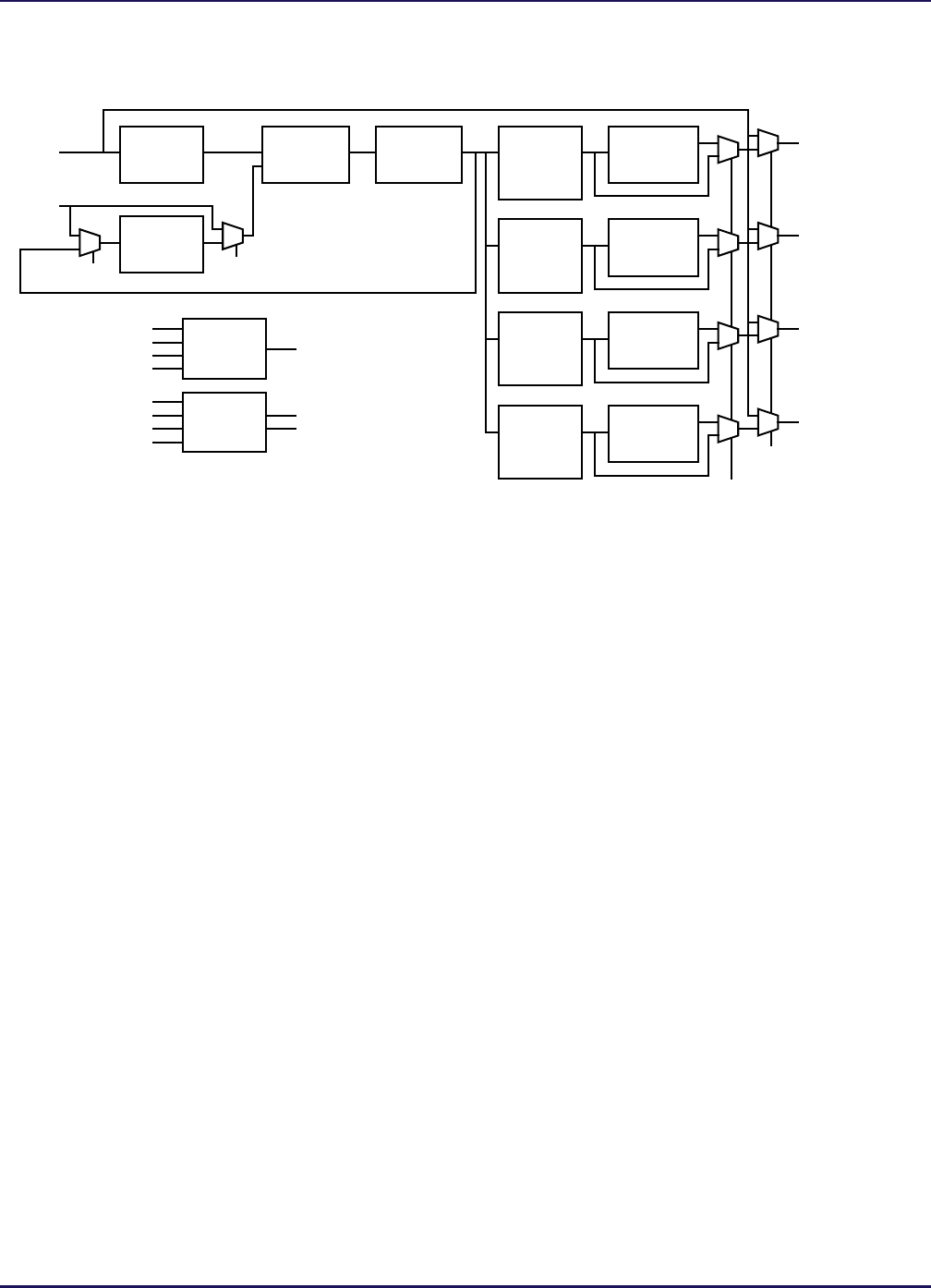
Figure 9-2: ACX_CLKGEN Block Diagram
ACX_CLKGEN Components
Reference Divider
The input reference clock can be divided by the Reference Divider. The Reference Divider
supportsvaluesfrom1to36andhasanoutputwitha50%dutycycle.Thefrequencyofthe
clockafteritpassesthroughthereferencedividermustbeintherangeof30MHzto400
MHz
forproperoperationofthePLL.
Voltage Controlled Oscillator (VCO)
TheACX_CLKGENmustbeconfiguredsothattheoutputoftheVoltageControlledOscillator
falls into the range of 1000 MHz to 2000 MHz. This is accomplished by programming the
Reference,FeedbackDivider, and OutputDividersuchthatthetwoclockinputstothePhase
FrequencyDetector arethesame and
fallwithinthe30MHzto400MHz range requiredby
thePhaseFrequencyDetector.
Phase Rotator with Output Divider
ThePhaseRotatorcanshifttheoutputclockphaseinincrementsof1/8thoftheinternalVCO
clock period at a time. The phase selection may be performed dynamically using the
phase_inc control input or the phase selection may be set to a static value by using the
static_phase parameter. The
phase selection of each of the four outputs may be set
independently.TheoutphrstninputallowsthefourPhaseRota torstobesimultaneouslyreset
tozerooffset.
TheOutputDividerprovidesa50%dutycycleoutputandsupportsdivisionratesfrom1to
63.TheOutputdividerdivisionratioissetindependentlyforeachofthefouroutputs.
Output Synthesizer
TheOutputSynthesizer allowstheusertodividetheoutputby (high_cnt+low_cnt),where
theratioofhigh_cntto(high_cnt+low_cnt)determinesthe outputdutycycle.
ACX_CLKGEN
Reference
Divider (M)
Phase
Frequency
Detector
Voltage
Controlled
Oscillator
Phase
Rotator w/
Output
Feedback
Divider (Q)
Output
Synthesizer
refclk
fbclk
clkout[3]
pll_lock
rstn
outphrstn
core_clken[3:0]
phase_inc[3:0]
ick_dspll_sif_clk
ick_dspll_sif_rstn
ick_sbus_data[1:0]
ick_sbus_req
ock_sbus_ack
ock_sbus_data[1:0]
Control
Serial
Interface
Phase
Rotator w/
Output
Phase
Rotator w/
Output
Phase
Rotator w/
Output
clkout[2]
clkout[1]
clkout[0]
intfb
phaseinc_sat
bypass[3:0]
high_cnt[3:0]
low_cnt[3:0]
Divider (N)
Divider (N)
Divider (N)
Divider (N)
0
1
1
0
(P)
Output
Synthesizer
(P)
Output
Synthesizer
(P)
Output
Synthesizer
(P)