
User Macro Guide
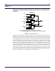
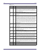
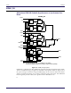
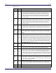
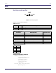
Table Of Contents
- Title - Speedster22i Macro Cell Library
- ChapterTitlePreface - Preface
- ChapterTitle - Chapter 1 – I/O Cells
- Table - Table 1-1: Supported Single-Ended Voltage Standards
- Table - Table 1-2: Supported Differential Voltage Standards
- Heading1 - IOPAD
- Heading1 - IOPAD_D
- Heading2 - Bidirectional Registered I/O Pad with Asynchronous or Synchronous Set/Reset
- Figure - Figure 1-2: IOPAD_D Logic Symbol
- Table - Table 1-7: Ports
- Table - Table 1-8: Parameters
- Table - Table 1-9: Output Function Table (txregmode = ”reg”, oeregmode = “reg”, rstmode = “async”)
- Table - Table 1-10: Output Function Table (txregmode = ”reg”, oeregmode = “reg”, rstmode = “sync”)
- Table - Table 1-11: Input Function table (rxregmode = “reg”)
- Heading3 - Verilog Instantiation Template
- Heading3 - VHDL Instantiation Template
- Heading2 - Bidirectional Registered I/O Pad with Asynchronous or Synchronous Set/Reset
- Heading1 - IOPAD_D2
- Heading2 - Bidirectional DDR I/O Pad with Asynchronous or Synchronous Set/ Reset
- Figure - Figure 1-3: IOPAD_D2 Logic Symbol
- Table - Table 1-12: Ports
- Table - Table 1-13: Parameters
- Figure - Figure 1-4: IOPAD_D2 Output Timing Diagram (assumes txdata_en = 1’b1)
- Figure - Figure 1-5: IOPAD_D2 Input Timing Diagram (assumes rxdata_en = 1’b1)
- Heading3 - Verilog Instantiation Template
- Heading3 - VHDL Instantiation Template
- Heading2 - Bidirectional DDR I/O Pad with Asynchronous or Synchronous Set/ Reset
- Heading1 - IPAD
- Heading1 - IPAD_D
- Heading1 - IPAD_D2
- Heading1 - IPAD_DIFF
- Heading1 - IPAD_DIFFD
- Heading1 - IPAD_DIFFD2
- Heading1 - OPAD
- Heading1 - OPAD_D
- Heading1 - OPAD_D2
- Heading1 - OPAD_DIFF
- Heading1 - OPAD_DIFFD
- Heading2 - Registered Differential Output Pad with Asynchronous or Synchronous Set/Reset
- Figure - Figure 1-19: OPAD_DIFFD Logic Symbol
- Table - Table 1-42: Ports
- Table - Table 1-43: Parameters
- Table - Table 1-44: Output Function Table (rstmode = “async”)
- Table - Table 1-45: Output Function Table (rstmode = “sync”)
- Heading3 - Verilog Instantiation Template
- Heading3 - VHDL Instantiation Template
- Heading2 - Registered Differential Output Pad with Asynchronous or Synchronous Set/Reset
- Heading1 - OPAD_DIFFD2
- Heading1 - TPAD
- Heading1 - TPAD_D
- ChapterTitle - Chapter 2 – Registers
- Heading1 - Naming Convention
- Heading1 - DFF
- Heading1 - DFFE
- Heading1 - DFFEC
- Heading1 - DFFEP
- Heading1 - DFFER
- Heading1 - DFFES
- Heading1 - DFFN
- Heading1 - DFFNEC
- Heading1 - DFFNEP
- Heading1 - DFFNER
- Heading1 - DFFNES
- Heading1 - DFFNR
- Heading1 - DFFNS
- Heading1 - DFFR
- Heading1 - DFFS
- ChapterTitle - Chapter 3 – Logic Functions
- ChapterTitle - Chapter 4 – Lookup Table (LUT) Functions
- ChapterTitle - Chapter 5 – Arithmetic Functions
- ChapterTitle - Chapter 6 – Memories
- Heading1 - BRAM80K
- Heading2 - 80k-bit Dual-Port Memory
- Heading2 - BRAM80K Pins
- Heading2 - Parameters
- Table - Table 6-2: BRAM80K Parameters
- Heading3 - porta_read_width(portb_read_width)
- Heading3 - porta_write_width(portb_write_width)
- Heading3 - porta_write_mode(portb_write_mode)
- Heading3 - porta_clock_polarity(portb_clock_polarity)
- Heading3 - porta_peval(portb_peval)
- Heading3 - porta_latch_rstval(portb_latch_rstval)
- Heading3 - porta_en_out_reg(portb_en_out_reg)
- Heading3 - porta_reg_rstval(portb_reg_rstval)
- Heading3 - porta_regce_priority(portb_regce_priority)
- Heading3 - porta_initval(portb_initval)
- Table - Table 6-3: Relationship of porta_initval(portb_initval) bit positions to douta,doutpa,doutpxa (doutb,doutpb,doutpxb)
- Heading3 - porta_srval(portb_srval)
- Table - Table 6-4: Relationship of porta_srval(portb_srval) bit positions to douta,doutpa,doutpxa (doutb,doutpb,doutpxb)
- Heading3 - mem_init_file
- Heading3 - initd_000 – initd_255
- Heading3 - initp_00 – initp_31
- Heading3 - initpx_00 – initpx_31
- Heading2 - Memory Organization and Data Input / Output Pin Assignments
- Table - Table 6-5: Valid Port A Width Versus Port B Width Combinations per port for n x 5 width modes
- Table - Table 6-6: Valid Port A Width Versus Port B Width Combinations per port for n x 9 width modes
- Table - Table 6-7: Valid Port A Width Versus Write Port B Combinations per port for n x 2 width modes
- Table - Table 6-8: dina(dinb) bit assignments per porta_write_width(portb_write_width) values
- Table - Table 6-9: Write Enable to Data Input Bus Mapping per Write Port Width
- Table - Table 6-10: douta(doutb) bit assignments per porta_read_width(portb_read_width) values
- Table - Table 6-11: BRAM80K Address Bus Mapping (Per Port)
- Table - Table 6-12: Mapping of Word Sizes to the Native 2048x40 Memory Locations
- Heading2 - Read and Write Operations
- Heading3 - Read Operation
- Heading3 - Write Operation
- Table - Table 6-13: BRAM Output Function Table for Latched Mode (Assumes active-high clock, port enable, and latch reset value)
- Table - Table 6-14: BRAM Output Function Table for Registered Mode (Assumes active-high clock, output register clock enable, and output register reset)
- Heading3 - Simultaneous Memory Operations
- Heading3 - Timing Diagrams
- Figure - Figure 6-3: Write-First, Latched Mode Timing Diagram
- Figure - Figure 6-4: Write-First, Registered Mode Timing Diagram
- Figure - Figure 6-5: No-Change, Latched Mode Timing Diagram
- Figure - Figure 6-6: No-Change, Registered Mode Timing Diagram
- Heading3 - Support for Read-First (Read-Before-Write) Memory Operations
- Heading2 - Memory Initialization
- Heading2 - BRAM80K Verilog Instantiation Template
- Heading2 - BRAM80K VHDL Instantiation Template
- Heading1 - BRAM80KFIFO
- Heading2 - 80k-bit FIFO Memory
- Heading2 - Parameters
- Table - Table 6-16: BRAM80KFIFO Parameters
- Heading3 - sync_mode
- Heading3 - write_width
- Table - Table 6-17: FIFO write_width versus Maximum Write Depth
- Table - Table 6-18: din, dinp, dinpx bit assignments per write_width values
- Heading3 - read_width
- Table - Table 6-19: FIFO read_width versus Maximum Read Depth
- Table - Table 6-20: dout bit assignments per read_width values
- Table - Table 6-21: Valid Read Width Versus Write Width Combinations per port for n x 5 width modes
- Table - Table 6-22: Valid Read Width Versus Write Width Combinations per port for n x 9 width modes
- Table - Table 6-23: Valid Read Width Versus Write Width Combinations per port for 2n width modes
- Heading3 - fwft
- Heading3 - en_out_reg
- Heading3 - reg_initval
- Table - Table 6-24: Relationship of reg_initval bit positions to dout,doutp,doutpx
- Heading3 - reg_srval
- Table - Table 6-25: Relationship of reg_srval bit positions to dout,doutp,doutpx
- Heading3 - reg_rstval
- Heading3 - wrrst_rstval
- Heading3 - wrrst_input_mode
- Table - Table 6-26: wrrst_input_mode Parameter Mapping.
- Figure - Figure 6-9: Read and Write Pointer Reset Input Selection Block Diagram
- Table - Table 6-27: Reset Usage Model for wrrst and rdrst Inputs
- Heading3 - wrrst_sync_stages
- Table - Table 6-28: Mapping wrrst_sync_stages Parameter Settings to Synchronization Stage Depth
- Heading3 - wrptr_sync_stages
- Table - Table 6-29: Mapping wrptr_sync_stages Parameter Settings to Synchronization Stage Depth
- Heading3 - rdrst_rstval
- Heading3 - rdrst_input_mode
- Table - Table 6-30: rdrst_input_mode Parameter Mapping.
- Heading3 - rdrst_sync_stages
- Table - Table 6-31: Mapping rdrst_sync_stages Parameter Settings to Synchronization Stage Depth
- Heading3 - rdptr_sync_stages
- Table - Table 6-32: Mapping rdptr_sync_stages Parameter Settings to Synchronization Stage Depth
- Heading3 - wrcount_sync_mode
- Heading3 - rdcount_sync_mode
- Heading3 - afull_offset
- Table - Table 6-33: Condition to Assert almost_full Flag based on afull_offset Parameter Assignment
- Heading3 - aempty_offset
- Table - Table 6-34: Condition to Assert almost_empty Flag based on afull_offset Parameter Assignment
- Heading3 - wren_polarity_sel
- Heading3 - rden_polarity_sel
- Heading3 - en_rd_when_empty
- Heading3 - en_wr_when_full
- Heading2 - Read and Write Count Outputs
- Heading2 - Status Flags
- Heading2 - Flag Latency
- Table - Table 6-35: FIFO Pointers and Status Flag Clock Domain Assignments
- Table - Table 6-36: Pointers Used for FIFO Flag Calculations
- Table - Table 6-37: Empty and Almost Empty Flag Latency in Terms of Read Clock Cycles
- Table - Table 6-38: Full and Almost Full Flag Latency in Terms of Write Clock Cycles
- Heading2 - Optional Output Register
- Heading2 - FIFO Operational Modes
- Heading2 - FIFO Operations
- Heading3 - Basic Mode FIFO Reset Operation
- Table - Table 6-40: Parameter Settings Required for Basic Mode FIFO Reset Operation
- Figure - Figure 6-12: Basic Mode FIFO Reset Timing Diagram
- Heading3 - Advanced Mode FIFO Reset Operation
- Figure - Figure 6-13: Reset Behavior Timing Diagram (Requires sync wrrst )
- Heading3 - Writing an Empty Asynchronous FIFO (sync_mode = 1’b0)
- Figure - Figure 6-14: Writing an Empty Asynchronous FIFO (sync_mode = 1’b0)
- Heading3 - Writing an Empty Synchronous FIFO (sync_mode = 1’b1)
- Figure - Figure 6-15: Writing an Empty Synchronous FIFO (sync_mode = 1’b1)
- Heading3 - Writing to an Almost Full FIFO (en_wr_when_full = 1’b0)
- Figure - Figure 6-16: Writing to an Almost Full FIFO (en_wr_when_full = 1’b0)
- Heading3 - Writing to an Almost Full FIFO (en_wr_when_full = 1’b1)
- Figure - Figure 6-17: Writing to an Almost Full FIFO (en_wr_when_full = 1’b1)
- Heading3 - Reading from an Almost Empty FIFO (en_rd_when_empty = 1’b0, fwft = 1’b0)
- Figure - Figure 6-18: Reading From an Almost Empty FIFO (en_rd_when_empty = 1’b0, fwft = 1’b0)
- Heading3 - Reading from an Almost Empty FIFO (en_rd_when_empty = 1’b0, fwft = 1’b1)
- Figure - Figure 6-19: Reading From an Almost Empty FIFO (en_rd_when_empty = 1’b0, fwft = 1’b1)
- Heading3 - Reading from an Almost Empty FIFO (en_rd_when_empty = 1’b1)
- Figure - Figure 6-20: Reading From an Almost Empty FIFO (en_rd_when_empty = 1’b1)
- Figure - Figure 6-21: Writing and Reading a Mixed-Width FIFO
- Heading3 - Limitations of Concurrent Read/Write Operations
- Heading1 - BRAM80KECC
- Heading2 - 80k-bit Simple Dual-Port Memory with Error Correction
- Heading2 - BRAM80KECC Pins
- Heading2 - Parameters
- Table - Table 6-42: BRAM80KECC Parameters
- Heading3 - en_out_reg
- Heading3 - reg_initval
- Table - Table 6-43: Relationship of reg_initval bit positions to dout,doutp,doutpx
- Heading3 - reg_srval
- Table - Table 6-44: Relationship of reg_srval bit positions to dout,doutp,doutpx
- Heading3 - reg_rstval
- Heading3 - encoder_enable
- Heading3 - decoder_enable
- Heading3 - mem_init_file
- Heading3 - initd_000 – initd_255
- Heading3 - initp_0 – initp_31
- Heading3 - initpx_0 – initpx_31
- Heading2 - BRAM80KECC Modes of Operation
- Heading2 - ECC Encode/Decode Operation Mode
- Heading2 - ECC Encode-Only Operation Mode
- Heading2 - ECC Decode-Only Operation Mode
- Heading1 - BRAM80KECCFIFO
- Heading1 - LRAM640
- Heading1 - LRAMFIFO
- Heading2 - LRAM-Based 64-Word FIFO Memory
- Heading2 - Parameters
- Table - Table 6-51: LRAMFIFO Parameters
- Heading3 - width
- Heading3 - depth
- Heading3 - ptr_sync_mode
- Heading3 - wrptr_sync_stages
- Table - Table 6-52: Mapping wrptr_sync_stages Parameter Settings to Synchronization Stage Depth
- Figure - Figure 6-33: Write Pointer Synchronizer Block Diagram
- Heading3 - rdptr_sync_stages
- Table - Table 6-53: Mapping rdptr_sync_stages Parameter Settings to Synchronization Stage Depth
- Figure - Figure 6-34: Read Pointer Synchronizer Block Diagram
- Heading3 - rst_sync_mode
- Heading3 - wrrst_sync_stages
- Table - Table 6-54: Mapping wrrst_sync_stages Parameter Settings to Synchronization Stage Depth
- Figure - Figure 6-35: Write Pointer Reset Input Selection Block Diagram
- Heading3 - rdrst_sync_stages
- Table - Table 6-55: Mapping rdrst_sync_stages Parameter Settings to Synchronization Stage Depth
- Figure - Figure 6-36: Read Pointer Reset Input Selection Block Diagram
- Heading3 - afull_offset
- Table - Table 6-56: Condition to Assert almost_full Flag based on afull_offset Parameter Assignment
- Heading3 - aempty_offset
- Table - Table 6-57: Condition to Assert almost_empty Flag based on aempty_offset Parameter Assignment
- Heading2 - Status Flags
- Heading2 - Flag Latency in Asynchronous Mode (ptr_sync_mode = 1’b0)
- Table - Table 6-58: FIFO Pointers and Status Flag Clock Domain Assignments
- Table - Table 6-59: Pointers Used for FIFO Flag Calculations (ptr_sync_mode = 1’b0)
- Table - Table 6-60: Empty and Almost Empty Flag Latency in Terms of Read Clock Cycles(ptr_sync_mode =1’b0)
- Table - Table 6-61: Full and Almost Full Flag Latency in Terms of Write Clock Cycles(ptr_sync_mode = 1’b0)
- Heading2 - Flag Latency in Synchronous Mode (ptr_sync_mode = 1’b1)
- Heading2 - FIFO Operational Modes
- Heading2 - FIFO Operations
- Heading3 - Asynchronous FIFO Mode Reset Operation
- Figure - Figure 6-37: Asynchronous FIFO Mode Reset Timing Diagram
- Heading3 - Writing an Empty Asynchronous FIFO (ptr_sync_mode = 1’b0)
- Figure - Figure 6-38: Writing an Empty Asynchronous FIFO (ptr_sync_mode = 1’b0)
- Heading3 - Writing an Empty Synchronous FIFO (ptr_sync_mode = 1’b1)
- Figure - Figure 6-39: Writing an Empty Synchronous FIFO (ptr_sync_mode = 1’b1)
- Heading3 - Writing to an Almost Full FIFO
- Figure - Figure 6-40: Writing to an Almost Full FIFO
- Heading3 - Reading from an Almost Empty FIFO
- Figure - Figure 6-41: Reading From an Almost Empty FIFO
- Heading1 - BRAM80K
- ChapterTitle - Chapter 7 – Multipliers
- Heading1 - BMACC56
- Heading2 - 28 x 28 Multiplier / Accumulator
- Heading2 - BMACC56 Pins
- Heading2 - Parameters
- Table - Table 7-3: BMACC56 Parameters
- Heading3 - init_a
- Heading3 - init_b
- Heading3 - init_sub
- Heading3 - init_cin
- Heading3 - init_mask_adda
- Heading3 - init_dout
- Heading3 - init_cout
- Heading3 - rst_value_a
- Heading3 - rst_value_b
- Heading3 - rst_value_sub
- Heading3 - rst_value_cin
- Heading3 - rst_value_mask_adda
- Heading3 - rst_value_dout
- Heading3 - rst_value_cout
- Heading3 - regce_priority_a
- Heading3 - regce_priority_b
- Heading3 - regce_priority_sub
- Heading3 - regce_priority_cin
- Heading3 - regce_priority_dout
- Heading3 - reg_a
- Heading3 - reg_b
- Heading3 - reg_addb
- Heading3 - reg_mask_adda
- Heading3 - reg_dout
- Heading3 - reg_cout
- Heading3 - sel_cascade_in
- Heading3 - sel_cascade_out
- Heading3 - sel_cin
- Table - Table 7-4: Add/Sub Block Carry Input Assignment
- Heading3 - sel_sub
- Table - Table 7-5: Add/Sub Block Sub Input Assignment
- Heading3 - mult_bypass
- Heading3 - clock_edge
- Heading2 - BMACC56 Verilog Instantiation Template
- Heading2 - BMACC56 VHDL Instantiation Template
- Heading1 - BMULT28X28
- Heading1 - BMACC56
- ChapterTitle - Chapter 8 – Special Functions
- ChapterTitle - Chapter 9 – PLL/DLL Clock Generators
- Heading1 - ACX_CLKGEN
- Heading2 - Phase-Locked Loop Clock Generator
- Heading2 - ACX_CLKGEN Pins
- Heading2 - Parameters
- Heading2 - ACX_CLKGEN Components
- Heading3 - Reference Divider
- Heading3 - Voltage Controlled Oscillator (VCO)
- Heading3 - Phase Rotator with Output Divider
- Heading3 - Output Synthesizer
- Heading3 - Phase Frequency Detector (PFD)
- Heading3 - Feedback Divider
- Heading3 - Clock Feedback Selection
- Table - Table 9-3: Clock Feedback Selection
- Heading3 - PLL Control
- Heading3 - Serial Control Bus (SCB)
- Figure - Figure 9-3: Serial Control Bus Read Operation
- Figure - Figure 9-4: Serial Control Bus Write Operation
- Heading2 - Control Status Registers (CSR) Register Description
- Heading1 - ACX_CLKGEN
- ChapterTitlePreface - Revision History

Table 1-7: Ports
Name Type Description
pad Bidirectional device pad.
din
Positive-edge based data input. I
f parameter txregmode=”reg”, data is
clocked into the din register upon the rising edge of the clk input, and is
driven to the pad if the oe input was high before the rising edge of the clk
input. If parameter txregmode=”nonreg”, din is driven to the pad when the
output is enabled (oe=1).
dout
Positive-edge based data output. I
f parameter rxregmode=”reg”, data is
clocked from the pad to dout on the rising edge of clk. If parameter rxreg-
mode=”nonreg”, the input register is b
ypassed and the pad is driven onto
output dout.
oe
Output Enable.
The output enable register transitions upon the rising edge
of the oeclk clock. A low value on the rstn input performs an asynchronous
clear to disable the output when the output enable is set to registered mode
by setting the oeregmode parameter to “reg”. A high value on oe enables the
output pad upon the next rising edge of the clock when the Output Enable
register is enabled. A low value on oe disables the pad upon the next rising
edge of the clock and places the pad in high impedance mode when the Out-
put Enable register is enabled. If the output ena
ble register is bypassed by
setting the txregmode parameter to “nonreg”, driving oe high immediately
enables the pad.
txdata_en
Output Register Clock Enable. A
high value on txdata_en enables the
Output Register to clock the din input to the output at the next rising edge
of the txclk. A low value on txdata_en allows the Output Register to retain
its current value.
rxdata_en
Input Register Clock Enable.
A high value on rxdata_en enables the
Input Register to clock the value on pad into the Input Register at the next
rising edge of the rxclk. A low value on rxdata_en allows the Input Regis-
ter to retain its current value.
txrstn
Output Register Asynchronous Reset. A
low value on txrstn performs an
asynchronous initialization of the Output Register. The value initialized
into the Output Register is determined by the value of the rstvalue param-
eter.
rxrstn
Input Register Asynchronous Reset. A low val
ue on rxrstn performs an
asynchronous initialization of the Input Register. The value initialized into
the Input Register is determined by the value of the rstvalue parameter.
oerstn
Output Enable Register Asynchr
onous Reset. A low value on oerstn per-
forms an asynchronous initialization of the Output Ena
ble Register and ini-
tializes it to a low value to put the
output in a high-impedance mode.
srstn
Synchronous Reset. A
low value on srstn performs a synchronous initial-
ization of the input register and output r
egister if the rstmode parameter is
set to "sync". Setting the rstmode parameter to "async" disables the syn-
chronous reset.
txclk Output Register Clock input for transmit side.
rxclk Input Register Clock input for receive side.
oeclk Output Enable Regist
er Clock input.
I/O Cells IOPAD_D
Speedster Macro Cell Library
www.achronix.com PAGE 5
inout
input
output
input
input
input
input
input
input
input
input
input
input