Acrosser Technology Co., Ltd. AR-B1894 Intel Pentium M Mini ITX Main Board User’s Manual V 1.2 Copyright© May., 2007. All rights reserved All other brand names are registered trademarks of their respective owners.
Copyright All rights reserved. The information contained in this guide has been validated and reviewed for accuracy. No patent liability is assumed with respect to the use of the information contained herein. While every precaution has been taken in the preparation of this guide, the Manufacturer assumes no responsibility for errors or omissions.
How to Use This Manual This manual is written for the system integrator, PC technician and knowledgeable PC end user. It describes how to configure your AR-B1894 to meet various operating requirements. The user’s manual is divided into four chapters, with each chapter addressing a basic concept and operation of the server board. Chapter 1: Introduction - presents what you have inside the box and gives you an overview of the product specifications and basic system architecture for the AR-B1894 server board.
Table of Content 1. INTRODUCTION..................................................................................................... 6 1.1 1.2 1.3 1.4 1.5 2. DESCRIPTION................................................................................................................................ 6 PACKING CHECK LIST................................................................................................................... 7 SPECIFICATIONS .........................................................
4.2.8 4.2.9 4.2.10 4.2.11 4.2.12 Frequency/Voltage Control ................................................................................................... 44 Load Fail-Safe Default ......................................................................................................... 44 Load Optimized Defaults ................................................................................................. 45 Supervisor/User Password Setting............................................................
1. Introduction 1.1 Description The AR-B1894 all-in-one Mini ITX is designed to fit a high performance Pentium M based processor and compatible for high-end computer system application with PCI bus architecture. It is made to meet today’s demanding pace, and keep complete compatibility with hardware and software designed for the IBM PC/AT. The on-board devices support one PCI slot, integrated graphics, and on-board three Marvell Gigabit Ethernet controllers.
1.2 Packing Check List The AR-B1894 package includes the following basic items accompany with this manual.
1.3 Specifications System FSB Supports Intel μFC-PGA 478 Pentium® M / Celeron® M Processor with 65nm / 90nm process technology, up to 2.26G / 2.
Audio Chipset Intel® ICH6M AC97 Codec Realtek ALC655 AC97 5.1 CH 3D audio interface Audio Interface Mic in, Line in, CD Audio in, Line out, Rear out and Center/Subwoofer out Ethernet Chipset Three Marvell® YukonTM-EC 88E8053 PCI ExpressTM Ethernet controllers Ethernet Interface IEEE 802.3 10/100/1000BASE-T Gigabit Ethernet compliant Mechanical & Environmental Power Type 3.3 V @ 3.
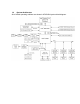
1.4 System Architecture All of details operating relations are shown in AR-B1894 system block diagram.
1.
2. Hardware Configuration Setting This chapter gives the definitions and shows the positions of jumpers, headers and connectors. All of the configuration jumpers on AR-B1894 are in the proper position. The default settings shipped from factory are marked with an asterisk ( ). In general, jumpers on the Mini ITX are used to select options for certain features. Some of the jumpers are designed to be user-configurable, allowing for system enhancement.
2.
IDE1 active LED (1-3) System power on LED (2-4) System reset LED (5-7) System power on switch LED (6-8) PCI1 PCI slot PWR1 24-pin ATX power connector SATA1, SATA2 Serial ATA 1 & 2 connector SPK1 Internal speaker connector SYS_FAN1 System fan connector USB1LAN1 USB 1, 2 & LAN 1 connectors USB2, USB3 Internal USB 3, 4 & 5, 6 connectors VGA_COM1 D-sub 15-pin VGA & D-sub 9-pin serial port 1 connectors 1 x 4 header 2 x 5 header
2.3 Jumpers/Connectors Setting 2.3.1 RTC CMOS Clear Select (JP1) OPEN Normal Operation SHORT Clear CMOS contents 2.3.3 Internal Audio for Chassis (AUDIO1) PIN No. 1 2 3 4 5 6 7 8 9 10 Description F_MIC1 Ground F_MIC2 +5V LOUTR F_R NC NC LOUTL F_L 2.3.5 CD-In from CD-ROM (CD1) PIN No. 1 2 3 4 Description CD-L CD-Ground CD-Ground CD-R 2.3.2 CPU Frequency Select (JP4) OPEN 400 MHz SHORT 533 MHz 2.3.4 Audio Connector (AUDIO2) PIN No.
2.3.7 COM1 / VGA & COM2 Connector (COM2, VGA_COM1) PIN No. 1 2 3 4 5 6 7 8 9 10 COM1 / COM2 Description Data Carrier Detect Received Data Transmit Data Data Terminal Ready Ground Data Set Ready Request To Send Clear To Send Ring Indicator Not used Description Green Signal NC Ground Ground Ground DCC_DATA VSYNC VGA PIN No. PIN No.
2.3.8 DVI Connector (DVI Description TDC0# TDC0 NC NC TDC1# TDC1 NC NC TDC2# TDC2 PIN No. 2 4 6 8 10 12 14 16 18 20 Signal Type TDC0,TDC0# O TDC1,TDC1# O TDC2,TDC2# O HPDET I TMDSDATA I/O TMDSDCLK I/O TLC,TLC# O PIN No. 1 3 5 7 9 11 13 15 17 19 Description +5V GND NC NC HPDET MDVIDATA MDVICLK Ground TLC# TLC Description DVI Data Channel 0 Output: These pins provide the DVI differential output for data channel 0 (Blue).
2.3.11 PS/2 Keyboard & Mouse (KBMS1) PIN No. 1 2 3 4 5 6 Description Keyboard Data Mouse Data Ground +5V Keyboard Clock Mouse Clock 2.3.12 LAN LED Connector (LAN_LED1) PIN No. 1 2 3 4 5 6 7 8 9 10 11 12 Description L1_LED_LINKACT L1_LED_LINK100 L1_LED_LINKACT_V L1_LED_LINK1000 L2_LED_LINKACT L2_LED_LINK100 L2_LED_LINKACT_V L2_LED_LINK1000 L3_LED_LINKACT L3_LED_LINK100 L3_LED_LINKACT_V L3_LED_LINK1000 2.3.13 LAN 1/2/3 & USB 1/2 Connectors (LAN2_LAN3, USB1LAN1) PIN No.
2.3.15 LVDS Connector (LVDS2) Description +5V +5V Ground LCTLB_CLK_L LCTLB_DATA_L Ground Ground A_CLKA_CLK+ Ground A_DATA0A_DATA0+ Ground A_DATA1A_DATAP+ Ground A_DATA2A_DATA2+ Ground +12V Signal PIN No. 2 4 6 8 10 12 14 16 18 20 22 24 26 28 30 32 34 36 38 40 PIN No. 1 3 5 7 9 11 13 15 17 19 21 23 25 27 29 31 33 35 37 39 Type Description +3.3V +3.
2.3.16 Front Side Indicators (PANEL1) PIN No. 1 3 PIN No. 5 7 PIN No. 6 8 2.3.17 24-pin ATX Power Connector (PWR1) Description +3.3V -12V Ground PS_ON Ground Ground Ground -5V +5V +5V +5V Ground IDE1 Active LED Signal Description +5V (Pull-up for HDD LED) HDD active# (LED cathode terminal) System Reset LED Signal Description Reset Ground System Power On Switch LED Signal Description Power button control signal Ground 2.3.18 Serial ATA 1/2 Connectors (SATA1, SATA2) PIN No.
3. System Installation This chapter provides you with instructions on how to setup your system. The additional information shows you how to install CPU/ FAN and memory. 3.1 Socket 478 Processors 3.1.1 Installing Intel® Pentium® M / Celeron® M CPU The processor socket comes with a screw to secure the processor, please unlock the screw first. Position the CPU above the socket and the gold triangular mark on the CPU must align with pin 1 of the CPU socket. Then Insert the CPU gently seated in place.
3.3 Main Memory AR-B1894 series provide 2 DIMMs (240-pin Dual In-line Memory Module) to support 1.5V DDRAM (Synchronized DRAM) as on-board main memory. The maximum memory size is 256 MB ~ 2 GB with using 256MB/512MB/1GB technology. Supports up to 2 double sided DIMMs at DDR2 533MHz. The memory architecture adopts 128-bit data interface to support for x8 and x16 DDRAM(DDR2) device width. In addition, it only supports Non-ECC memory.
3.4 Installing the Mini-ITX To install your AR-B1894 into standard chassis or proprietary environment, you need to perform the following steps: 1. Check all jumpers setting on proper position 2. Install and configure CPU and memory module on right position 3. Place AR-B1894 into the dedicated position in your system 4. Attach cables to existing peripheral devices and secure it NOTE: Please refer section 3.4 to install display and Ethernet drivers and setup your system.
3.4.2 Triple Marvell Gigabit Ethernet Controller Triple Marvell Gigabit Ethernet 10/100/1000BASE-TX controller by PCI Express. The AR-B1894 series provide three LED indicators on RJ-45 connectors to show LAN interface status. These messages will give you a guide for troubleshooting. LAN1: Yellow LED indicates transmit and receive activity.
4. BIOS Setup 4.1 Entering Setup Phoenix-Award BIOS has a built-in setup program that allows users to modify the basic system configuration. This information is stored in CMOS RAM whose power is supplied by a battery so that it can retain the setup information even when the power is turned off. Press Delete when you Power on or Reboot the computer system. (i.e. After the logo appears at the center of the screen, please press Delete to enter the BIOS setup program).
4.2.1Standard CMOS Features 4.2.1.1 Date (mm/date/year) and Time (hh/mm/ss) Allow you to change the date and time of the system clock. No matter how good the quality of the motherboard, remember that losing (or gaining) several seconds per month is not a surprising thing. 4.2.1.2 IDE Channel 0 Master/Slave You can press Enter to see the submenus they contain. 4.2.1.3 Video Allows you to select the type of displaying standard you are using. Available options are EGA/VGA, CGA 40, CGA 80 and MONO. 4.2.1.
4.2.2Advanced BIOS Features 4.2.2.1 CPU Feature 4.2.2.1.1 Delay Prior to Thermal Select the delay thermal time.
4.2.2.1.2 Thermal Management This BIOS feature controls the activation of the Thermal Monitor’s automatic mode. It allows you to determine when the Pentium M4’s Thermal Monitor should be activated in automatic mode after the system boots. In general, the Thermal Monitor should not be activated immediately on booting since the processor will be under a heavy load during the booting process, which results in the sharp rise in die temperature from its cold state, which leads to the unstable system.
4.2.2.2 Hard Disk Boot Priority Select removable device priority, such as Pri.Master, Pri,Slave, USBHDD0, USBHDD1, USBHDD2, and Bootable Add-in Cards. 4.2.2.3 Virus Warning Allows to choose the VIRUS warning feature for IDE Hard Disk boot sector protection. If this function is enabled and someone attempts to write data into this area, BIOS will show a warning message on screen and alarm beep. 4.2.2.4 CPU L1 & L2 Cache Cache memory is much faster than conventional DRAM system memory.
4.2.2.8 Boot Up NumLock Status This function defines the keyboard's numberpad as number keys or arrow keys. If it is set at On the number keys will be activated, if it is set at Off the arrow keys will be activated. 4.2.2.9 Typematic Rate Setting When enabled, you can set the following two-typematic control items. When disabled, the keyboard controller determines keystrokes arbitrarily in your system. 4.2.2.
4.2.3Advanced Chipset Features 4.2.3.1 DRAM Timing Selectable This item determines DRAM clock/timing using SPD or manual configuration. Make sure your memory module has SPD (Serial Presence Data), if you want to select the “By SPD” option. Options: Manual、By SPD (default) 4.2.3.2 CAS Latency Time CAS is short for column address strobe, which is a kind of signals. When the CPU needs data from SDRAM, CAS signals will be sent via the CAS line to specify the column where the data is needed.
4.2.3.4 DRAM RAS# Precharge This item allows you to select the DRAM RAS# precharge time. The ROW address strobe must precharge again before DRAM is refreshed. An inadequate configuration may result in incomplete data. This field is adjustable only when “DRAM Timing Selectable” is set to “manual”. This field is locked when “DRAM Timing Selectable” is set to “By SPD” and is automatically determined by the system. Options: 5、4、3、2. 4.2.3.
4.2.3.13 Panel Scaling This item is for the backlight scaling techniques dynamically dimming the backlight to conserve its power consumption as increasing the panel transmittance to maintain the same luminance. Most displays use either spatial or temporal method to synthesize colors. 4.2.3.14 Panel Number This item allows to select panel resolution that will be displayed depending on the LCD panel (LFP).
4.2.4Integrated Peripheral 4.2.4.1 Onchip IDE Device 4.2.4.3.1 IDE HDD Block Mode Block mode is also called block transfer, multiple commands, or multiple sector read/write. If the IDE hard drive supports block mode (most new drives do), select Enabled for automatic detection of the optimal number of block read/writes per sector the drive can support. 4.2.4.3.
4.2.4.3.3 On-Chip Primary/Secondary PCI IDE The chipset contains a PCI IDE interface with support for two IDE channels. Select Enabled to activate the primary IDE interface. Select Disabled to deactivate this interface. 4.2.4.3.4 IDE Primary/Secondary Master/Slave PIO The IDE PIO (Programmed Input/Output) fields let you set a PIO mode (0-4) for each of the four IDE devices that the onboard IDE interface supports. Modes 0 through 4 provide successively increased performance.
4.2.4.2 Onboard Device 4.2.4.3.1 USB Controller This item allows you to set the USB Controller. 4.2.4.3.2 USB 2.0 Controller This item allows you to set the USB 2.0 Controller. 4.2.4.3.3 USB Keyboard Support This item allows you to set the system’s USB keyboard to Enabled/Disabled. 4.2.4.3.4 USB Mouse Support This item allows you to set the system’s USB Mouse to Enabled/Disabled. 4.2.4.3.
4.2.4.3 Super IO Device 4.2.4.3.1 Onboard Serial Port 1/2 Select Enabled if your system has a floppy disk controller (FDC) installed on the system board and you wish to use it. If you are not going to use FDC or the system has no floppy drive, select Disabled in this field. 4.2.4.3.2 UART Mode Select Select an address and corresponding interrupt for the first and second serial ports. 4.2.4.3.3 RxD,TxD Active This BIOS feature allows to set the infra-red reception (RxD) and transmission (TxD) polarity.
4.2.5Power Management Setup 4.2.5.1 ACPI Function This function enables PCs to implement Power Management functions through Operating System and also provides the opportunity to integrated the interface for controlling power management and Plug-n-Play features on system devices. 4.2.5.2 ACPI Suspend Type This item allows to set the ACPI suspend(sleep) mode instead of simply turning off a computer.
4.2.5.3 Run VGABIOS if S3 Resume This item is to select whether to run VGABIOS if resumed from S3 state but for older VGA drivers only. Please select Auto (Default) if in doubt. 4.2.5.4 Power Management There are three selections for power management and HDD power down. The Min. Power Saving sets the HDD Power Down at 15 Min., Max. Power Saving at 1 Min., and User defined from 1 Min. to 15 Min. and disabled but from 1 Min. to 1 hour while disabled. 4.2.5.
4.2.6PnP/PCI Configurations 4.2.6.1 Init Display First This item allows you to decide to active whether PCI Slot or Onboard/AGP first. 4.2.6.2 Reset Configuration Data Normally, you leave this field Disabled. Select Enabled to reset Extended System Configuration Data (ESCD) when you exit Setup if you have installed a new addon and the system reconfiguration has caused such a serious conflict that the operating system cannot boot. 4.2.6.
4.2.6.3.1 IRQ Resources This item allows you to determine the IRQ assigned to the ISA bus and is not available to any PCI slot. Legacy ISA for devices compliant with the original PC AT bus specification, PCI/ISA PnP for devices compliant with the Plug and Play standard whether designed for PCI or ISA bus architecture. 4.2.6.3.2 DMA Resources This item allows you to determine the DMA assigned to the ISA bus and is not available to any PCI slot.
4.2.6.4 PCI/VGA Palette Snoop This function determines if the graphics card should allow VGA palette snooping by a fixed function display card. It is only useful if a fixed-function display card using that requires a VGA-compatible graphics card to be present. Otherwise, leave the setting as default Disabled. 4.2.6.5 Maximum Payload This item allows to set the maximum TLP payload size (unit in byte) for the PCI Express devices. 4.2.7PC Health Status 4.2.7.
4.2.8Frequency/Voltage Control 4.2.8.1 Auto Detect PCI/DIMM Clk This item allows to enable/disable auto detect PCI/DIMM clock. 4.2.8.2 Spread Spectrum This is to adjust extreme value of the pulse for EMI test. 4.2.9Load Fail-Safe Default Use this menu to load the BIOS default values for the minimal/stable performance for your system to operate. Press to load the BIOS default values for the most stable, minimalperformance system operations.
4.2.10 Load Optimized Defaults Use this menu to load the BIOS default values that are factory settings for optimal performance system operations. While Award has designed the custom BIOS to maximize performance, the factory has the right to change these defaults to meet their needs. Press to load the default values setting for optimal performance system operations. 4.2.11 Supervisor/User Password Setting You can set either supervisor or user password, or both of them.
User Password: able to enter but no right to change the options of setup menus. Type the password, up to eight characters in length, and press . The password typed now will clear any previously entered password from CMOS memory. You will be asked to confirm the password. Type the password again and press . You may also press to abort the selection and not enter a password. To disable a password, just press when you are prompted to enter the password.
4.2.12 Exit Selection Save CMOS value changes to CMOS and exit setup. Enter to store the selection made in the menus in CMOS, a special section in memory that stays on after turning the system off. The BIOS configures the system according to the Setup selection stored in CMOS when boot the computer next time. The system is restarted after saving the values.