
Instruction Manual
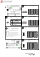
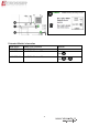
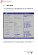
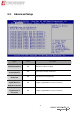

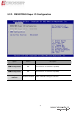
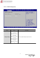

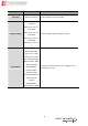
Table Of Contents
- Chapter 1 Introduction
- Chapter 2 Procedures of Assembly/Disassembly
- Chapter 3 Board Introduction
- Chapter 4 H/W Information
- Chapter 5 BIOS Settings
- SATA Configuration
- W83627DHG Super IO Configuration
- Serial Port Console Redirection
- Intel(R) 82576 Gigabit Dual Port Network Connection
- N/A
- Configure Gigabit Ethernet device parameters
- Intel(R) 82574L Gigabit Network Connection
- N/A
- Configure Gigabit Ethernet device parameters
- SATA Mode Selection
- Port 1
- Port 2
- CF card
- COM1 Configuration
- COM2 Configuration
- LAN by Pass Function
- Change Settings
- Serial Port
- Change Settings
- Device Mode
- Console Redirection
- Console Redirection Settings
- EMS
- EMS Settings
- Terminal Type
- Bits per second
- Data Bits
- Parity
- Stop Bits
- Flow Control
- NIC Configuration
- Blink LEDs (range 0-1
- Link Status
- NIC Configuration
- Blink LEDs (range 0-1
- Link Status
- SYS temperature
- CPU temperature
- CPU Fan Speed
- VCORE
- LAN1 ~ 8
- USB Configuration
- xHCI Mode
- EHCI1
- Setup Prompt Timeout
- Boot up NumLock State
- Boot Logo
- PXE Function
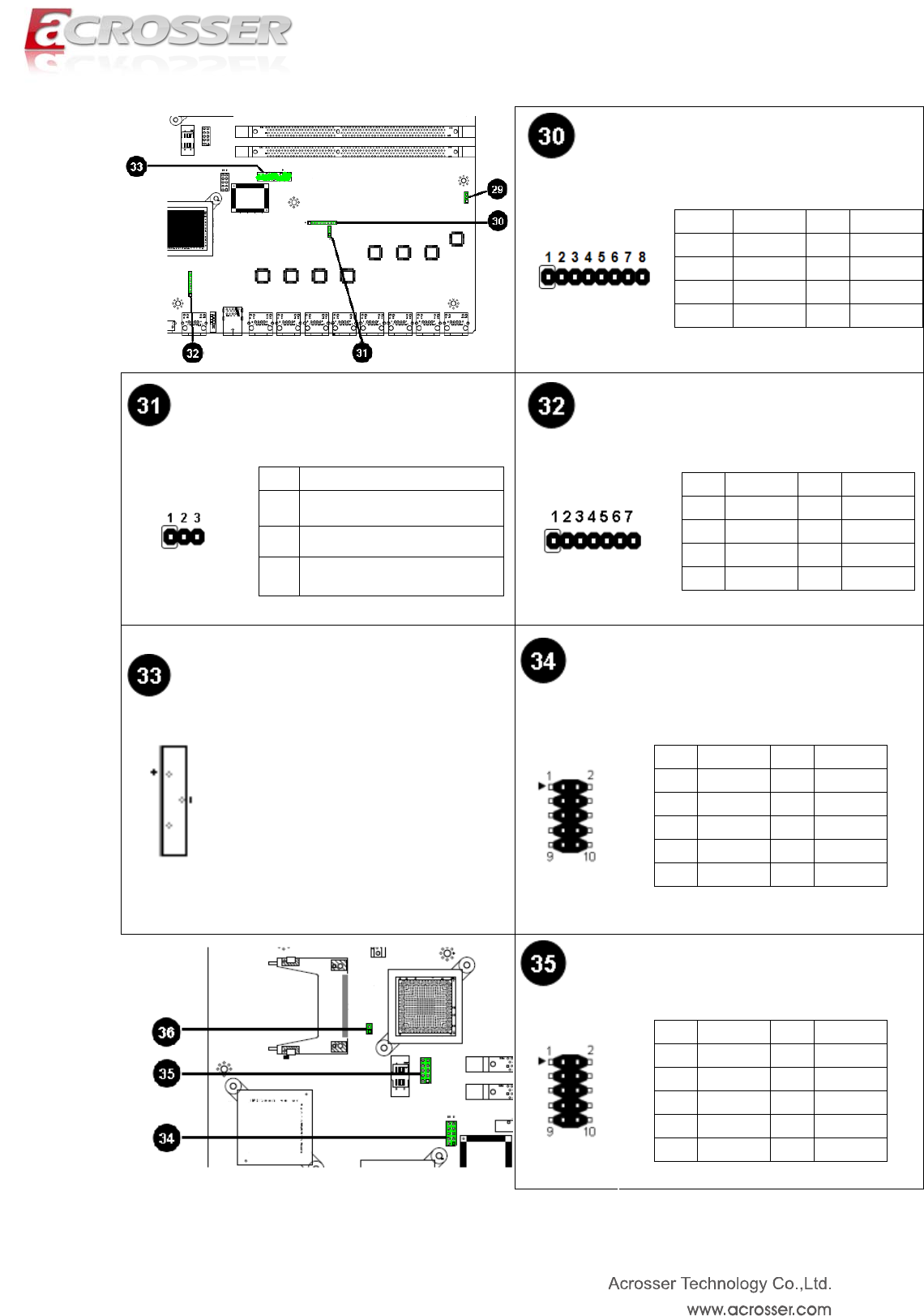
CPLD1
For CPLD Firmware Update
PIN Signal PIN Signal
1 3VDUAL 2 G_TDO
3 G_TDI 4 NC
5 NC 6 G_TMS
7 GND 8 G_TCK
JP4
(For LAN3/LAN4 Bypass Function
Select.).
LCM1
LCM signal connector
PIN Function
1-2 Forced Normal (Default)
2-3 Controlled By CPLD
Ope
n
Forced Bypass
PIN Signal PIN Signal
1 3VDUAL 2 G_TDO
3 G_TDI 4 NC
5 NC 6 G_TMS
7 GND 8 G_TCK
LPC1 LPC Header For Port’80 Debug
RTC1
CMOS Backup Battery:
An onboard battery saves the CMOS
memory to keep the BIOS information
stays on even after disconnected
your system with power source. Nevertheless,
this backup battery exhausts after
some five years.
PIN Signal PIN Signal
1 33MHz 2 LAD1
3 Reset 4 LAD0
5 FRAME# 6 VCC3
7 LAD3 8 GND
9 LAD2 10 GND
SPI1
SPI BIOS firmware Update
Header
PIN Signal PIN Signal
1 CS0 2 VCC3
3 MISO 4 HOLD#
5 WP# 6 SPICLK
7 GND 8 MOSI
9 NC 10 NC
31