AR-B1047 SOLID STATE DISK CARD User’s Guide Edition: 1.5 Book Number: AR-B1047-02.
AR-B1047 User’s Guide Table of Contents 0. PREFACE ...........................................................................................................................................................0-2 0.1 0.2 0.3 0.4 0.5 0.6 0.7 1. COPYRIGHT NOTICE AND DISCLAIMER......................................................................................................................... 0-2 WELCOME TO THE AR-B1047 ROM CARD .............................................................................
AR-B1047 User’s Guide 0.PREFACE 0.1 COPYRIGHT NOTICE AND DISCLAIMER August 1998 This document is copyrighted, 1998, by Acrosser Technology Co., Ltd. All rights are reserved. No part of this manual maybe reproduced, copied, transcribed, stored in a retrieval system, or translated into any language or computer language in any form or by any means, such as electronic, mechanical, magnetic, optical, chemical, manual or other means without prior written permission of original manufacturer.
AR-B1047 User’s Guide 0.6 ORGANIZATION This information for users covers the following topics (see the Table of Contents for a detailed listing): ! ! ! ! ! ! ! Chapter 1, “Overview”, provides an overview of the system features and packing list. Chapter 2, “Setting Up the System”, describes how to adjust the jumpers and the connectors setting. Chapter 3, “Installation”, describes setup procedures including information on the utility diskette.
AR-B1047 User’s Guide 1. OVERVIEW This chapter provides an overview of your system features and capabilities. The following topics are covered: ! ! ! Introduction Packing List Features 1.1 INTRODUCTION This card is a byte wide memory card that plugs into any free slot of your system. Five 32-pin JEDEC DIP sockets may be populated with up to 5MB of EPROM, 2.5MB of FLASH/SRAM or combinations of these chips. Especially AR-B1047, it supports up to 72MB DiskOnChip. The AR-B1047 supports 12V and 5V FLASHs.
AR-B1047 User’s Guide 1.2 PACKING LIST The accessories are included with the system. Before you begin installing your AR-B1047 board, take a moment to make sure that the following items have been included inside the AR-B1047 package. ! ! ! ! This user’s guide 1 AR-B1047 solid state disk card 1 Screws bag 1 Software utility CD 1.
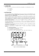
AR-B1047 User’s Guide 2. SETTING UP THE SYSTEM This chapter describes pin assignments for the system’s external connectors and jumper settings. ! ! ! ! Overview System Setting DIP Switch Setting Memory Type Setting 2.1 OVERVIEW This section provides the AR-B1047 hardware’s jumpers setting, the connectors’ locations, and the pin assignment.
AR-B1047 User’s Guide 2.2 SYSTEM SETTING Jumper pins allow you to set specific system parameters. Set them by changing the pin location of jumper blocks. (A jumper block is a small plastic-encased conductor [shorting plug] that slips over the pins.) To change a jumper setting, remove the jumper from its current location with your fingers or small needle-nosed pliers. Place the jumper over the two pins designated for the desired setting. Press the jumper evenly onto the pins.
AR-B1047 User’s Guide 2.2.2 PC/104 Connector (1) 64 Pin PC/104 Connector Bus A & B (CN1) 64 2 1 63 64-Pin PC/104 Connector Figure 2-4 CN1: 64-Pin PC/104 Connector Bus A & B CN1 1 2 N.C. --SD7 --SD6 --SD5 --SD4 --SD3 --SD2 --SD1 --SD0 --N.C.
AR-B1047 User’s Guide 2.3 DIP SWITCH SETTING (SW1) There is 1-DIP Switch located on the AR-B1047. If you want to use the 12V FLASH, please use the external 12V voltage, the AR-B1047 does not support the 12V voltage.
AR-B1047 User’s Guide 2.3.3 SSD Drive Number (SW1-3 & SW1-4) The AR-B1047’s SSD can simulate one or two disk drives. You can assign the drive letter of the AR-B1047 by configuring SW1-3 & SW1-4. You can make the computer to boot from SSD by copying DOS into the SSD. If your SSD does not have DOS, the computer will boot from your hard disk or floppy disk. In this condition, the SSD BIOS of AR-B1047 will set the drive letter of the SSD to the desired drive letter automatically.
AR-B1047 User’s Guide (2) Disk Drive Name Arrangement If any logical hard disk drives exist in your system, there will also be a different disk number, which is depending on version DOS you are using. The solid-state disk drive number with the respective DOS drive designation are listed in table as follows. Floppy disk No.
AR-B1047 User’s Guide 2.4 MEMORY TYPE SETTING (M1, M2 & M3) Before installing the memory into memory sockets MEM1 through MEM5, you have to configure the memory type, which will be used (ROM/RAM) on the AR-B1047. You can configure the AR-B1047 as an EPROM (FLASH) disk (ROM only), a SRAM disk (SRAM only) or a combination of EPROM (FLASH) and SRAM disk. It is not necessary to insert memory chips into all of the sockets. The number of SRAM chips required depends on your RAM disk capacity.
AR-B1047 User’s Guide 3. INSTALLATION The chapter describes the various type SSDs’ installation steps as follows. The jumper and switch adjust as SSD’s different type to set. ! ! ! ! ! Overview ROM Disk Installation Using the Write Protect Function Memory Device Supported How to Use the D.O.C. CAUTION: When the power is turned off, please note the following precautions. 1. If your data has been stored in the SRAM disk, do not change the jumper position or data will be lost. 2.
AR-B1047 User’s Guide To execute PGM1047.EXE, the main menu will be displayed on your screen. There are 8 options on the main menu. Quit to DOS Quits and exits to the DOS. OS Shell Exits from PGM1047 temporarily to the DOS prompt. Type EXIT to return to PGM1047 main menu. Load ROM File If this option is used, the PGM1047 will prompt you for the ROM pattern file name. This option is useful if you have not previously entered a ROM pattern file name or if you wish to use a different ROM pattern file.
AR-B1047 User’s Guide (C) RFG.EXE RFG.EXE This program is used to generate ROM pattern files in a binary format. Each ROM pattern file has the same size as the FLASH or EPROM and can be easily programmed on to the FLASH with onboard programmer or on to EPROM with any EPROM programmer. If you have specified a DOS drive in the *.PGF file, RFG will generate bootable ROM pattern files for the EPROM or FLASH disk. The RFG supports the following DOS: MS-DOS, PC-DOS, DR-DOS, and X-DOS.
AR-B1047 User’s Guide (D) RFGDEMO.PGF RFGDEMO.PGF This file provides a sample PROGRAM GROUP FILE which illustrates how to create ROM pattern files correctly. The PGF is an ASCII text file that can be created by using any text editor, word processor or DOS command. The PGF lists what files will be copied and if DOS is going to be copied. This file can have any DOS filename, but the extension name must be *.PGF. For example, followings are valid filenames. RFGDEMO.PGF MYRFG.PGF MSDOS.
AR-B1047 User’s Guide 3.2.1 UV EPROM (27Cxxx) (1) Switch and Jumper Setting Step 1: Use jumper block to set the memory type as ROM (FLASH). Step 2: Use jumper JP1 to select the correct EPROM type if 1Mx8 (27C080) EPROM is used. Step 3: Select the proper I/O base port, firmware address, disk drive number and EPROM type on SW1. Step 4: Insert programmed EPROM(s) or FLASH(s) chips into sockets starting at MEM1. Step 5: Line up and insert the AR-B1047 card into any free slot of your computer.
AR-B1047 User’s Guide Step 8: Install EPROM chips Be sure to place the programmed EPROMs (R01, R02…) into socket starting from MEM1 and ensure that the chips are installed in the sockets in the proper orientation. 3.2.2 12V or Large Page 5V FLASH Disk If you are using 12V FLASH or large page 5V FLASH as ROM disk, you have to followed the same procedure as step 1 to step 4 by using the UV EPROM.
AR-B1047 User’s Guide A B C 1 JP1 2 1 2 3 4 5 3 M1, M2, & M3 A B 5V/12V FLASH (64KX8, 128KX8 and 256KX8) (Factory Preset) C JP1 1 2 1 2 3 4 5 3 M1, M2, & M3 5V FLASH (512KX8 Only) Figure 3-5 M1~M3 & JP1-3~JP1-5: 12V or Large Page 5V FLASH Jumper Setting (2) Software Programming And then, you should create a PGF and generate ROM pattern files by using the RFG.EXE. Step 1: Making a Program Group File (*.
AR-B1047 User’s Guide 3.2.3 Small Page 5V FLASH ROM Disk (1) Switch and Jumper Setting Step 1: Use jumper block to set the memory type as ROM (FLASH). Step 2: Use jumper JP1 to select the correct EPROM type. Step 3: Select the proper I/O base port, firmware address, disk drive number and EPROM type on SW1. Step 4: Insert programmed EPROM(s) or FLASH(s) chips into sockets starting at MEM1. Step 5: Line up and insert the AR-B1047 card into any free slot of your computer.
AR-B1047 User’s Guide (3) Typing DOS Command You can use another way to format and copy files to the 5V FLASH EPROM. This method provides the convenience of using a RAM disk. You can use the DOS and command to format and copy files. Follow the steps to format and copy files to the FLASH disk. It is the same procedure as step 1 to step 4 of using the UV EPROM.
AR-B1047 User’s Guide (2) Software Programming It is very easy to use the RAM disk. The RAM disk operates just like a normal floppy disk. A newly installed RAM disk needs to be formatted before files can be copied to it. Use the DOS command [FORMAT] to format the RAM disk. Step 1: Use jumper block to select the memory type as SRAM refer. Step 2: Select the proper I/O base port, firmware address and disk drive number on SW1.
AR-B1047 User’s Guide 3.3 USING THE WRITE PROTECT FUNCTION The AR-B1047 provides software write protect functions for small page 5V FLASH disk and only software write protect function for SRAM disk to prevent your data on 5V FLASH or SRAM disk from accidental deletion or overwrite.
AR-B1047 User’s Guide 3.4 MEMORY DEVICE SUPPORTED Five 32-pin JEDEC memory sockets on the AR-B1047 can be populated with up to 5MB of EPROM, 2.5MB of FLASH, 2.5MB of SRAM or combinations the EPROM/SRAM or FLASH/SRAM.
AR-B1047 User’s Guide 4. HOW TO USE THE MEMORY BANKS This section provides the information about how to access the memory on the AR-B1047 without using the ARB1047 SSD BIOS. The AR-B1047 hardware cut every 8K bytes of memory into a memory bank. To access the data in memory, you have to assign the chip number and the bank number. On every chip, the memory bank number starts from the number zero. The last memory bank number depends on the size of the memory chip used on the AR-B1047.
AR-B1047 User’s Guide 5. SPECIFICATIONS & SSD TYPE SUPPORTED 5.1 SPECIFICATIONS Bus Interface: PC/104 bus Memory Socket: Five 32-pin JEDEC sockets for SSD One socket for DiskOnChip EPROM – 5MB maximum FLASH – 2.5MB maximum SRAM – 2.5MB maximum DOC – 72MB maximum 27C010 (128Kx8), 27C020 (256Kx8), 27C040 (512Kx8), and 27C080 (1Mx8) Disk Capacity: EPROM Type: FLASH Type: SRAM Type: Battery: Disk Drive: Occupy Memory: From 64Kx8 to 512Kx8 FLASH chips.
AR-B1047 User’s Guide AMD Am29F040 (512Kx8, 4M bits) The following list contains small page 5V FLASHs supported by the AR-B1047: ATMEL AT29C512 (64Kx8, 512K bits) SST PH29EE512 (64Kx8, 512K bits) ATMEL AT29C010 (128Kx8, 1M bits) SST 28EE010 (128Kx8, 1M bits) SST 28EE011 (128Kx8, 1M bits) SST PH29EE010 (128Kx8, 1M bits) WINBOND W29EE011 (128Kx8, 1M bits) ATMEL AT29C020 (256Kx8, 2M bits) ATMEL AT29C040 (512Kx8, 4M bits) ATMEL AT29C040A (512Kx8, 4M bits) SST PH28SF040 (512Kx8, 4M bits) The following list co
AR-B1047 User’s Guide 6. PLACEMENT & DIMENSIONS 6.
AR-B1047 User’s Guide 6.2 DIMENSIONS 350 2900 1050 200 3150 3550 Unit: mil (1 inch = 25.
AR-B1047 User’s Guide 7. INDEX Name CN1 CN2 J1 SW1 JP1-1 & JP1-2 JP1-3~JP1-5 M1, M2, & M3 Function 64 pin PC/104 connector bus A & B 40 pin PC/104 connector bus C & D External Battery Header I/O port, memory and SSD select Battery Charge Select 1Mx8 EPROM select Memory type select Page 2-3 2-3 2-2 2-4 2-2 2-7 2-7 Note: If the content in Setting is inconsistent with the CD-ROM, please refer to Setting as the priority.