AR-B1790 INDUSTRIAL GRADE CPU BOARD User’ s Guide Edition: 1.03 Book Number: AR-B1790-03.
Table of Contents 0. PREFACE............................................................................................................................................... 2 0.1 COPYRIGHT NOTICE AND DISCLAIMER .....................................................................................................................................2 0.2 WELCOME TO THE AR-B1790 CPU BOARD................................................................................................................................
0. PREFACE 0.1 COPYRIGHT NOTICE AND DISCLAIMER This document is copyrighted, 2002, by Acrosser Technology Co., Ltd. All rights are reserved. No part of this manual may be reproduced, copied, transcribed, stored in a retrieval system, or translated into any language or computer language in any form or by any means, such as electronic, mechanical, magnetic, optical, chemical, manual or other means without the prior written permission or original manufacturer.
0.6 STATIC ELECTRICITY PRECAUTIONS Before removing the board from its anti-static bag, read this section about static electricity precautions. Static electricity is a constant danger to computer systems. The charge that can build up in your body may be more than sufficient to damage integrated circuits on any PC board. It is, therefore, important to observe basic precautions whenever you use or handle computer components.
1. INTRODUCTION Welcome to the AR-B1790 Embedded ATX Single Board Computer. The AR-B1790 board is Embedded ATX form factor board, which comes equipped with high performance Intel® Pentium 4 Processor with the Intel® advanced chipset the Intel® 845GV GMCH and ICH4 (Intel® 82801DB). This product is designed for the system manufacturers, integrators, or VARs that want to provide all the performance, reliability, and quality at a reasonable price. In addition, the AR-B1790 provides on chip VGA.
1.2 PACKING LIST In addition to this User's Manual, the AR-B1790 package includes the following items: The quick setup manual AR-B1790 Embedded ATX Single Board Software utility CD x 1 FDD Cable x 1 (Optional) 5.25” IDE HDD ATA 100Cable x 1(Optional) 2.
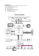
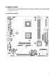
2. INSTALLATION This chapter describes how to install the AR-B1790. At first, the layout of AR-B1790 is shown, and the unpacking information that you should be careful is described. The jumpers and switches setting for the AR-B1790’s configuration are as below. 2.
7
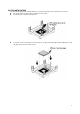
2.2 CPU INSTALLATION This main board supports Intel Pentium 4/Celeron, Socket 478 series CPU. Please follow the step as below: Be careful of CPU orientation when you plug it into CPU socket. Pull up the CPU socket lever and up to 90° Locate Pin 1 in the socket and look for a black dot or cut edge on the CPU upper interface. Match Pin 1 and cut edge, then insert into the CPU socket.
Press down the CPU socket lever and finish CPU installation. The Intel Pentium 4/Celeron processor requires a set of heatsink/fan to ensure proper cooling of processor. If heatsink/fan have not been already bundled with your CPU, you must purchase the heatsink/fan separately and have it installed. Plug the cable through the heatsink/fan in the CPU fan power connector located nearby. Note that there are seceral types of CPU fan connector.
3. CONNECTION This chapter describes how to connect peripherals, switches and indicators to the AR-B1790 board. 3.1 IDE DISK DRIVE CONNECTOR (IDE1, IDE2) • IDE1: Primary IDE Connector A 40-pin header type connector (IDE1) is provided to interface with up to two embedded hard disk drives (IDE AT bus). This interface, through a 40-pin cable, allows the user to connect up to two drives in a “daisy chain” fashion.
• IDE 2: Second IDE Connector AR-B1790 also provides IDE interface 44-pin connector to connect with the hard disk device. 2 44 1 43 Pin 1 3 5 7 9 11 13 15 17 19 21 23 25 27 29 31 33 35 37 39 41 43 Signal -RESET DATA 7 DATA 6 DATA 5 DATA 4 DATA 3 DATA 2 DATA 1 DATA 0 GROUND SDDREQ -SOIOW -SOIOR SIORDY -SDDACK IRQ15 SDA1 SDA0 -SDCS1 HLEDS VCC GROUND Pin 2 4 6 8 10 12 14 16 18 20 22 24 26 28 30 32 34 36 38 40 42 44 Signal GROUND DATA 8 DATA 9 DATA 10 DATA 11 DATA 12 DATA 13 DATA 14 DATA 15 N.
3.
3.
3.6 USB CONNECTOR (USB1, USB2, USB3) USB1&USB2 5 6 7 8 1.VCC 5.VCC 2.DATA0+ 6.DATA1+ 3.DATA0- 7.DATA11 2 3 4 USB 3 2 1 10 9 4.GND 1.VCC 2.GND 3.DATA24.GND 5.DATA2+ 8.GND 6.DATA3+ 7.GND 8.DATA39.GND 10.VCC 3.7 FAN POWER CONNECTOR The AR-B1790 provides CPU cooling Fan connector. CPU connectors can supply 12V/500mA to the cooling fan. 3 2 1 FAN1 FOR CPU FAN FAN2 FOR SYSTEM FAN FAN3 FOR CASE FAN PIN 1 2 3 Signal GND +12V SENSE 3.
3.9 PARALLEL & COM1 & VGA PORT (PT1) AR-B1790 built-in a 9-pin standard COM port, a 15-pin VGA port and 1 LPT port. Device like printer can de connected to LPT port . Mouse and modem etc can de connected to COM port. CRT monitor can be connected to VGA port.
3.11 GPIO PORT (GPIO1) PIN 1 3 5 7 9 11 13 15 17 19 21 23 25 DEFINE GPI0 GPI1 GPI7 GPI12 GPI13 GPI33 GPI34 GPI35 GPI36 GPI37 GPI38 GPI39 GPI_1 PIN 2 4 6 8 10 12 14 16 18 20 22 24 26 DEFINE GPO16 GPO17 GPO18 GPO19 GPO20 GPO21 GPO22 GPO23 GPO24 GPO25 GPO27 GPO40 GPO41 27 29 31 33 GPI_2 GPI_3 GPI_4 VCC5V 28 30 32 34 GPO42 GPO43 GPO_1 GND 3.12 ATX POWER CONNECTOR (PWR1) Pin 1 2 3 4 5 6 7 8 9 10 1 10 11 20 Signal 3.3V 3.
3.14 DUAL LVDS CONNECTOR (LVDS1, LVDS2) 2 26 1 25 LVDS1 PIN 1 2 3 4 5 6 7 8 9 10 11 12 13 Signal TXOUT0GND TXOUT0+ GND TXOUT1LVDSVCC TXOUT1+ LVDSVCC TXOUT2N.C TXOUT2+ GND TXCLK1- PIN 14 15 16 17 18 19 20 21 22 23 24 25 26 Signal GND TXCLK1+ VTX12 TXOUT3VTX12 TXOUT3+ GND VTKBP N.C LVDSVCC N.C LVDSVCC N.C PIN 1 2 3 4 5 6 7 8 9 10 11 12 13 Signal TXOUT4GND TXOUT4+ GND TXOUT5LVDSVCC TXOUT5+ LVDSVCC TXOUT6N.
3.15 LVDS PANEL VOLTAGE SELECT (JP8) 1 2 5 6 JP8 1-3 2-4 ON 3-5 4-6 ON VOLTAGE +5V +3.3V (Factory Preset) 3.16 CONTROL LVDS PANEL BACK-LIGHT (JP9) PIN 1 2 3 3 2 1 Signal +12V GND EBLT 3.17 COM VOLTAGE SELECT (JP11, JP12, JP13) 1 2 5 6 PIN Signal PIN Signal 1 COM VOLTAGE 2 +12V 3 COM VOLTAGE 4 +5V 5 COM VOLTAGE 6 GND (Factory Preset) ﹡JP11 SELECT COM1 PIN 10 VOLTAGE ﹡ ﹡JP12 SELECT COM2 PIN 10 VOLTAGE ﹡ ﹡JP13 SELECT COM3 PIN 10 VOLTAGE ﹡ 3.
3.21 CLEAR CMOS (JP6) JP6 1 1-2 ON 3 2-3 ON FUNCTION Normal Operation (Factory Preset) Clear CMOS 3.22 FRONT PANEL (JP7) PIN 1 3 5 7 9 11 13 15 17 19 21 2 22 1 21 Signal 5VSUS POWER BUTTON N.C GREEN BUTTON GND N.C VCC PRIMARY HDD ACT LED VCC SECONDARY N.C PIN 2 4 6 8 10 12 14 16 18 20 22 Signal VCC POWER LED N.C 5VSB SUSPEND LED N.C 5V EXTERNAL SPEAKER N.
3.23 COMPACT FLASH (CF1) 50 1 Compact Flash (CF1) and IDE 2 share the same channel. Since a Compact Flash card is installed in the socket, the IDE 2 device will become unusable. CF card & IDE2 device cannot use at the same time. 3.24 GAME/MINI PORT AND AUDIO CONNECT The connector supports joystick, MINI Keyboard and other relate audio device.
3.25 CD-IN CONNECTOR (CD-IN) The connector is for CD-ROM audio connector PIN 1 2 3 4 1 4 Signal CD_L GND GND CD_R 3.26 CPU SPEED SELECT (JP5) JP5 1 1-2 SPEED CPU SELECT (Factory Preset) 2-3 100MHz EMPTY 133MHz 3 3.27 CF VOLTAGE SELECT (JP23) 1 JP23 VOLTAGE 2 1-2 +3.3V 3 2-3 +5V Factory Preset 3.
4. WATCHDOG TIMER This section describes the use of Watchdog Timer, including disable, enable, and trigger. AR-B1790 is equipped with a programmable time-out period watchdog timer that occupies I/O port 443H. Users can use simple program to enable the watchdog timer. Once you enable the watchdog timer, the program should trigger it every time before it times out. Watchdog Timer will generate a response (system or IRQ9) due to system fails to trigger or disable watchdog timer before preset timer, times out.
5. BIOS CONSOLE This chapter describes the AR-B1790 BIOS menu displays and explains how to perform common tasks needed to get up and running, and presents detailed explanations of the elements found in each of the BIOS menus. The following topics are covered: BIOS Setup Overview Standard CMOS Setup Advanced CMOS Setup Advanced Chipset Setup Power Management PCI/Plug and Play Peripheral Setup Auto-Detect Hard Disks Password Setting Load Default Setting BIOS Exit 5.
CAUTION: 1. AR-B1790 BIOS the factory-default setting is used to the Acrosser recommends using the BIOS default setting, unless you are very familiar with the setting function, or you can contact the technical support engineer. 2. If the BIOS settings are lost, the CMOS will detect the to boot the operation system, this option will reduce the performance of the system.
Primary/Secondary Master/Slave Press PgUp/<+> or PgDn/<-> to select Manual, None or Auto type. Note that the specifications of your drive must match with the drive table. The hard disk will not work properly if you enter improper information for this category. If your hard disk drive type is not matched or listed, you can use Manual to define your own drive type manually. If you select Manual, related information is asked to be entered to the following items.
1st/2nd/3rd Boot Device The items allow you to set the sequence of boot devices where BIOS attempts to load the disk operating system. The settings are: Floppy LS120 HDD-0 CDROM HDD-1 HDD-2 HDD-3 ZIP LAN Disabled The system will boot from floppy drive. The system will boot from LS-120 drive. The system will boot from the first HDD. The system will boot from the CD-ROM. The system will boot from the second HDD. The system will boot from the third HDD. The system will boot from the fourth HDD.
L2 Cache This option specifies the caching algorithm used for L2 secondary (external) cache memory. 5.4 ADVANCED CHIPSET SETUP This option controls the configuration of the board’s chipset. Control keys for this screen are the same as for the previous screen. Advanced Chipset Setup DRAM Frequency PC-200 means the memory bus is running at 200MHz. PC-266 means the memory bus is running at 266MHz. The Choice: 200Mhz, 266Mhz Configure SDRAM Timing by SPD SPD is the abbreviation Serial Presence Detect.
Internal Graphics Mode Select - Shares 512K/1MB/8MB of the system memory in DOS mode - Uses Dynamic Video Memory Technology (DVMT) in Windows mode USB Controller This option can enable USB Port 0&1or Disabled USB function. USB1.1 Device Legacy Support These options are used to Enabled the USB function and it’s only useful in the DOS mode. The USB function sets Enabled will occupy IRQ10. Boot Display Device Use the field to select the type of device you want to use as the display(s) of the system.
Mouse PowerOn Function When set to [Enabled], this parameter allows you to use the PS/2 mouse to turn on the system. This feature requires an ATX power supply that provides at least 1A on the +5VSB lead. Configuration options: [Disabled] [Left-button] [Right-button] ACPI Standby State This option will not be shown or not be available if you are using a CPU with the locked ratio. Auto: BIOS will automatically select ACPI Suspend type S1/POS:Set ACPI Suspend type to S1.
Init. Graphics Adapter Priority Internal VGA PCI / Int-VGA Clear NVRAM This sets the operating mode of the boot block area of the BIOS FLASH ROM to allow programming in the Yes setting. 5.7 PERIPHERAL SETUP This section is used to configure peripheral features. Peripheral Setup OnBoard IDE This option is to set up the operating mode of IDE controller. If the main board offers the enhanced I/O port, the choice should be .
IR Duplex Mode This setting controls the operating mode of IR transmission/reception. Setting options: Full, Half. Under Full Duplex mode, synchronous, bi-directional transmission/reception is allowed. Under Half Duplex mode, only asynchronous, i-directional transmission/reception is allowed. IR Pin Select Please consult your IR peripheral documentation to select the correct setting of the TxD and RxD signals. Setting options: RxD2,TxD2, IR-Rx2Tx2.
5.10.1 Auto Configuration with Optimal Setting The user can load the optimal default settings for the BIOS. The Optimal default settings are best-case values that should optimize system performance. If CMOS RAM is corrupted, the optimal settings are loaded automatically. Load high performance setting (Y/N) ? 5.10.2 Auto Configuration with Fail Safe Setting The user can load the Fail-Safe BIOS Setup option settings by selecting the Fail-Safe item from the Default section of the BIOS Setup main menu.
APPENDIX A. ADDRESS MAPPING IO Address Map I/O MAP 000-01F 020-021 022-023 040-05F 060-06F 070-07F 080-09F 0A0-0BF 0C0-0DF 0F0-0FF 1F0-1F7 170-177 2E8-2EF 2F8-2FF 378-37F 3B0-3DF 3E8-3EF 3F0-3F7 3F8-3FF ASSIGNMENT DMA controller (Master) Interrupt controller (Master) Chipset controller registers I/O ports. Timer control registers.
APPENDIX B.