
Data Sheet

© 2005 Microchip Technology Inc. DS21984A-page 9
MCP73831
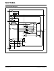
3.0 PIN DESCRIPTION
The descriptions of the pins are listed in Table 3-1.
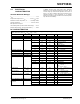
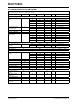
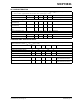
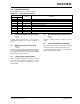
TABLE 3-1: PIN FUNCTION TABLES
3.1 Battery Management Input Supply
(V
DD
)
A supply voltage of [V
REG
(typ.) + 0.3V] to 6V is
recommended. Bypass to V
SS
with a minimum of
4.7 μF.
3.2 Battery Charge Control Output
(V
BAT
)
Connect to positive terminal of battery. Drain terminal
of internal P-channel MOSFET pass transistor. Bypass
to V
SS
with a minimum of 4.7 μF to ensure loop stability
when the battery is disconnected.
3.3 Charge Status Output (STAT)
STAT is a tri-state logic output for connection to an LED
for charge status indication. Alternatively, a pull-up
resistor can be applied for interfacing to a host
microcontroller.
3.4 Battery Management 0V Reference
(V
SS
)
Connect to negative terminal of battery and input
supply.
3.5 Current Regulation Set (PROG)
Preconditioning, fast charge, and termination currents
are scaled by placing a resistor from PROG to V
SS
.
The charge management controller can be disabled by
allowing the PROG input to float.
Pin No.
Symbol Function
DFN SOT23-5
14 V
DD
Battery Management Input Supply
2— V
DD
Battery Management Input Supply
33 V
BAT
Battery Charge Control Output
4— V
BAT
Battery Charge Control Output
5 1 STAT Charge Status Output
62 V
SS
Battery Management 0V Reference
7 — NC No Connection
8 5 PROG Current Regulation Set and Charge Control Enable