
Datasheet

16-Bit
ADC
DS
I C
Interface
2
Voltage
Reference
Oscillator
ALERT/RDY
SCL
SDA
ADDR
Gain=2/3, 1,
2,4,8,or16
PGA
Comparator
ADS1115
AIN1
AIN2
GND
AIN0
AIN3
VDD
MUX
ADS1113
ADS1114
ADS1115
SBAS444B –MAY 2009–REVISED OCTOBER 2009
www.ti.com
OVERVIEW
of a differential, switched-capacitor ΔΣ modulator
The ADS1113/4/5 are very small, low-power, 16-bit,
followed by a digital filter. Input signals are compared
delta-sigma (ΔΣ) analog-to-digital converters (ADCs).
to the internal voltage reference. The digital filter
The ADS1113/4/5 are extremely easy to configure
receives a high-speed bitstream from the modulator
and design into a wide variety of applications, and
and outputs a code proportional to the input voltage.
allow precise measurements to be obtained with very
little effort. Both experienced and novice users of The ADS1113/4/5 have two available conversion
data converters find designing with the ADS1113/4/5 modes: single-shot mode and continuous conversion
family to be intuitive and problem-free. mode. In single-shot mode, the ADC performs one
conversion of the input signal upon request and
The ADS1113/4/5 consist of a ΔΣ analog-to-digital
stores the value to an internal result register. The
(A/D) core with adjustable gain (excludes the
device then enters a low-power shutdown mode. This
ADS1113), an internal voltage reference, a clock
mode is intended to provide significant power savings
oscillator, and an I
2
C interface. An additional feature
in systems that only require periodic conversions or
available on the ADS1114/5 is a programmable digital
when there are long idle periods between
comparator that provides an alert on a dedicated pin.
conversions. In continuous conversion mode, the
All of these features are intended to reduce required
ADC automatically begins a conversion of the input
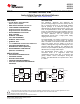
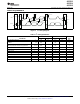
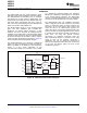
external circuitry and improve performance. Figure 22
signal as soon as the previous conversion is
shows the ADS1115 functional block diagram.
completed. The rate of continuous conversion is
equal to the programmed data rate. Data can be read
The ADS1113/4/5 A/D core measures a differential
at any time and always reflect the most recent
signal, V
IN
, that is the difference of AIN
P
and AIN
N
. A
completed conversion.
MUX is available on the ADS1115. This architecture
results in a very strong attenuation in any
common-mode signals. The converter core consists
Figure 22. ADS1115 Functional Block Diagram
10 Submit Documentation Feedback Copyright © 2009, Texas Instruments Incorporated
Product Folder Link(s): ADS1113 ADS1114 ADS1115