
Datasheet
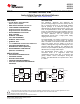
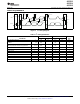

ADS1113
ADS1114
ADS1115
SBAS444B –MAY 2009–REVISED OCTOBER 2009
www.ti.com
This integrated circuit can be damaged by ESD. Texas Instruments recommends that all integrated circuits be handled with
appropriate precautions. Failure to observe proper handling and installation procedures can cause damage.
ESD damage can range from subtle performance degradation to complete device failure. Precision integrated circuits may be more
susceptible to damage because very small parametric changes could cause the device not to meet its published specifications.
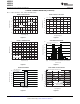
ORDERING INFORMATION
For the most current package and ordering information, see the Package Option Addendum at the end of this
document, or see the TI web site at www.ti.com.
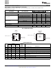
ABSOLUTE MAXIMUM RATINGS
(1)
ADS1113, ADS1114, ADS1115 UNIT
VDD to GND –0.3 to +5.5 V
Analog input current 100, momentary mA
Analog input current 10, continuous mA
Analog input voltage to GND –0.3 to VDD + 0.3 V
SDA, SCL, ADDR, ALERT/RDY voltage to GND –0.5 to +5.5 V
Maximum junction temperature +150 °C
Storage temperature range –60 to +150 °C
(1) Stresses above those listed under Absolute Maximum Ratings may cause permanent damage to the device. Exposure to absolute
maximum conditions for extended periods may affect device reliability.
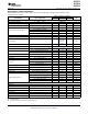
PRODUCT FAMILY
PACKAGE INPUT CHANNELS
DESIGNATOR RESOLUTION MAXIMUM SAMPLE (Differential/
DEVICE MSOP/QFN (Bits) RATE (SPS) COMPARATOR PGA Single-Ended)
ADS1113 BROI/N6J 16 860 No No 1/1
ADS1114 BRNI/N5J 16 860 Yes Yes 1/1
ADS1115 BOGI/N4J 16 860 Yes Yes 2/4
ADS1013 BRMI/N9J 12 3300 No No 1/1
ADS1014 BRQI/N8J 12 3300 Yes Yes 1/1
ADS1015 BRPI/N7J 12 3300 Yes Yes 2/4
2 Submit Documentation Feedback Copyright © 2009, Texas Instruments Incorporated
Product Folder Link(s): ADS1113 ADS1114 ADS1115