
Datasheet
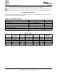
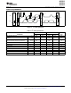
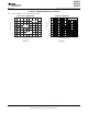

300
250
200
150
100
50
0
OperatingCurrent( A)m
-40 -20 0 20 40 60 80 100 120 140
Temperature(°C)
VDD =5V
VDD =2V
VDD =3.3V
5.0
4.5
4.0
3.5
3.0
2.5
2.0
1.5
1.0
0.5
0
ShutdownCurrent( A)m
-40 -20 0 20 40 60 80 100 120 140
Temperature(°C)
VDD =5V
VDD =2V
VDD =3.3V
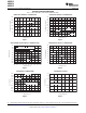
150
100
50
0
50
100
150
200
250
300
-
-
-
-
-
-
OffsetError( V)m
-40 -20 0 20 40 60 80 100 120 140
Temperature( C)°
VDD=2V
FS= 4.096V±
(1)
FS= 2.048V±
FS= 1.024V±
FS= 0.512V±
VDD=5V
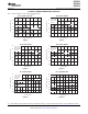
60
50
40
30
20
10
0
10
20
-
-
OffsetVoltage( V)m
-40 -20 0 20 40 60 80 100 120 140
Temperature(°C)
VDD =3V
VDD =2V
VDD =5V
VDD =4V
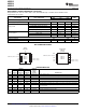
0.05
0.04
0.03
0.02
0.01
0
0.01
0.02
0.03
0.04
-
-
-
-
GainError(%)
-40 -20 0 20 40 60 80 100 120 140
Temperature(°C)
FS= 0.512V±
FS= 0.256V±
FS= 1.024V, 2.048V,
4.096V ,and 6.144V
± ±
± ±
(1) (1)
0.15
0.10
0.05
0
0.05
0.10
0.15
-
-
-
GainError(%)
2.0 2.5 3.0 3.5 4.0 4.5 5.0 5.5
SupplyVoltage(V)
FS= 256mV±
FS= 2.048V±
ADS1113
ADS1114
ADS1115
SBAS444B –MAY 2009–REVISED OCTOBER 2009
www.ti.com
TYPICAL CHARACTERISTICS
At T
A
= +25°C and VDD = 3.3V, unless otherwise noted.
OPERATING CURRENT vs TEMPERATURE SHUTDOWN CURRENT vs TEMPERATURE
Figure 2. Figure 3.
SINGLE-ENDED OFFSET ERROR vs TEMPERATURE
(1)
DIFFERENTIAL OFFSET vs TEMPERATURE
Figure 4. Figure 5.
GAIN ERROR vs TEMPERATURE GAIN ERROR vs SUPPLY
Figure 6. Figure 7.
(1) This parameter expresses the full-scale range of the ADC scaling. In no event should more than VDD + 0.3V be applied to this device.
6 Submit Documentation Feedback Copyright © 2009, Texas Instruments Incorporated
Product Folder Link(s): ADS1113 ADS1114 ADS1115