Adafruit Capacitive Touch Sensor Breakouts Created by Bill Earl Last updated on 2014-12-11 11:45:16 AM EST
Guide Contents Guide Contents 2 Overview 4 Momentary 5 Toggle 6 5-Pad Momentary 6 Assembly and Wiring 8 Installing the Headers: 8 Position the header strips 8 Position the breakout 8 And Solder 9 Wiring for Toggle and Momentary 10 Toggle Operation 11 Momentary Operation 12 Other Options: 12 LED Control 13 Speed vs. Power (Momentary Only) 13 Timer (Toggle Only) 14 Connecting to your Circuit.
Install the Panel 27 And Test 28 Connect to your Circuit 29 Downloads © Adafruit Industries https://learn.adafruit.
Overview These breakout boards are a simple way to add capacitive touch to your project. Just power with 1.8 to 5.5VDC and touch the pad to activate the sensor. These touch switches interface easily to any project - with or without a microcontroller. When a capacitive load (such as a human hand) is in close proximity to the sense-pad, the sensor detects the change in capacitance and activates the switch.
Momentary This sensor has a built-in sense-pad and is active for as long as the sensor area is touched. The sense-pad can be extended with wire and almost any conductive material. © Adafruit Industries https://learn.adafruit.
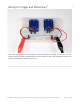
Toggle This sensor also has a built-in sense-pad. It becomes active when touched and remains active until it is touched again. As with the momentary sensor, the sense-pad can be extended with wire and almost any conductive material. 5-Pad Momentary This version combines 5 momentary switches into one breakout. There are 5 pins for attaching wires to up to 5 external sensor pads. © Adafruit Industries https://learn.adafruit.
We also have a new 12-Key version with it's own tutorial over here! (http://adafru.it/dKH) © Adafruit Industries https://learn.adafruit.
Assembly and Wiring These breakouts come fully assembled. For use in a breadboard, you may want to take a couple minutes to install the included header strips: Installing the Headers: Install the headers by following these 3 easy steps. The photographs below show one of each sensor type. Position the header strips Plug them long-pins down into a breadboard to stabilize them for soldering. Position the breakout Place the breakout board over the header pins. © Adafruit Industries https://learn.adafruit.
And Solder Solder each pin for solid electrical contact. © Adafruit Industries https://learn.adafruit.
Wiring for Toggle and Momentary These two breakouts are very similar and can be powered by anything from 1.8V to 5.5V DC. Simply connect Ground to GND and the positive voltage to VDD. The standalone sensors are fully functional without further connections. © Adafruit Industries https://learn.adafruit.
Toggle Operation The Toggle version of the sensor turns on when you touch it once, then turns off when you touch it again. The on-board LED indicates the state of the switch. © Adafruit Industries https://learn.adafruit.
Momentary Operation The momentary touch sensor works just like a momentary switch. It is on when you touch it and off when you move away. The on-board LED indicates the state of the switch. Other Options: These sensors have several jumper configurable operating modes as described below: © Adafruit Industries https://learn.adafruit.
LED Control The led indicators can be disabled for ultra-low power applications. To disable the LED, simply cut the jumper between the pads where indicated on the back of the breakout board. With the jumper cut, the LED can be controlled externally via the LED pin on the header. Speed vs. Power (Momentary Only) The Momentary version can be configured for "Fast" mode (default) or low-power mode. Fast mode requires 0.5mA. Low Power mode requires just 50uA.
Timer (Toggle Only) By default, the toggle sensor is configured for infinte time-out. it will stay on until you touch the sensor to turn it off. It also supports a configurable time-out to turn off the output automatically after a delay. To select this mode, cut the 'TIMER' jumper and connect a resistor & capacitor to the TIME pin. For a circuit diagram and resistor/capacitor calculations, see page 13 of the datasheet (http://adafru.it/cgW).
Simple Motor Control You can use it just like a pushbutton or logic signal with a transistor or MOSFET to drive highcurrent loads like a DC motor. © Adafruit Industries https://learn.adafruit.
Wiring for 5-pad Momentary The 5-pin momentary breakout can be powered with anything from 1.8V to 5.5VDC. Just connect ground to GND and the positive voltage to VDD. This sensor does not have built-in touch pads, but you can create your own pads in any size or shape from wire, foil or any other conductive material. Simply connect your touch-pads to each of the 5 sense pins. When you touch the pad, the corresponding LED on the other side will light up.
© Adafruit Industries https://learn.adafruit.
Adding Custom Touch Pads Custom touch pads are easy to make. You can use almost any conductive material: © Adafruit Industries https://learn.adafruit.
Wire, Thread, Foil, Fabric, Paint If it will conduct electricity, it will work as a touch sensor! © Adafruit Industries https://learn.adafruit.
© Adafruit Industries https://learn.adafruit.
Connections: The Toggle and Momentary boards have a solder hole located just below the sensor pad for attaching a wire to an external sensor. The 5-pad breakout has pins numbered 0-4 on the left side of the board. © Adafruit Industries https://learn.adafruit.
Sensor Pads Attach the connecting wire to any conductive object or surface. That surface will become touch sensitive. Larger surfaces tend to be more sensitive. You will be able to sense through fabric, plastic glass and many other non-conductive materials. Note that the wire will be touch sensitive too! Be sure to route any connecting wires away from areas where they might create an accidental touch input. © Adafruit Industries https://learn.adafruit.
Build a Touch Control Panel Capacitive touch sensors are a great way to add external controls to a waterproof enclosure. There is no need to drill holes or worry about gaskets and O-rings. These sensors will detect your touch right through the plastic case! Design your panel You can draw it by hand, or with your favorite drawing tool and print it on some heavy cardstock. © Adafruit Industries https://learn.adafruit.
Cut the touch-pads Cut pads from copper tape. About 1/2" square is a good size for buttons on a touch-pad. Attach the touch-pads Peel the release paper from the back of the copper tape and stick the touch-pads to be back of the panel so that they align with the buttons on the front. © Adafruit Industries https://learn.adafruit.
Attach the Wires Solder wires to the copper touch-pads. For this example, I used a 6-conductor 0.1" socket cable (http://adafru.it/206) with one end cut off to simplify connections to the breakout. © Adafruit Industries https://learn.adafruit.
Adjust the Wires Bend the wires away from the panel. The wires will be touch-sensitive too. To prevent accidental false touches, we want to keep them away from the panel surface. © Adafruit Industries https://learn.adafruit.
Install the Panel Tape the panel to the inside of the polycarbonate cover using clear packing tape. © Adafruit Industries https://learn.adafruit.
And Test Connect the cable to the breakout. Power it up and test your control panel. Touching each button should cause a different LED to light up. © Adafruit Industries https://learn.adafruit.
Connect to your Circuit The output signals are 'active low', so they can replace any pushbutton that shorts to ground such as the buttons on the RGB LCD shield. You can leave off the buttons and solder directly to the circled pads, or (if your shield is already built), just 'tack-solder' the wires to the legs of the buttons. When you put it all together, you will have a completely sealed, touch sensitive control panel! © Adafruit Industries https://learn.adafruit.
© Adafruit Industries https://learn.adafruit.
Downloads Schematics for '1010 and '1012 breakouts (click to enlarge) © Adafruit Industries https://learn.adafruit.
© Adafruit Industries Last Updated: 2014-12-11 11:45:20 AM EST Page 32 of 32
Features • Configurations: • • • • • • • • • • • • • – Comms mode – Standalone mode Number of Keys: – Comms mode – 1 to 7 keys (or 1 to 6 keys plus a Guard Channel) – Standalone mode – 1 to 4 keys plus a fixed Guard Channel on key 0 Number of I/O Lines: – Standalone mode – 5 outputs Technology: – Patented spread-spectrum charge-transfer Key Outline Sizes: – 6 mm x 6 mm or larger (panel thickness dependent); widely different sizes and shapes possible Layers Required: – One Electrode Materials: – Etc
1. Pinouts and Schematics 1.1 1.
AT42QT1070 1.3 Pinout Configuration – Comms Mode (20-pin VQFN) N/C N/C N/C KEY5 KEY6 20 19 18 17 16 KEY4 1 15 SCL KEY3 2 14 CHANGE KEY2 3 13 RESET KEY1 4 12 SDA KEY0 5 QT1070 6 8 9 11 10 MODE (Vss) N/C Vdd Vss N/C N/C 1.
1.5 Pin Descriptions Table 1-1. Pin 1 2 4 Pin Listings (14-pin SOIC) Name (Comms Mode) Name (Standalone Mode) Type Vdd Vdd P Power – I Mode selection pin Comms Mode – connect to Vss Standalone Mode – connect to Vdd – MODE (Vss) MODE (Vdd) 3 SDA OUT0 OD 4 RESET RESET I Description If Unused, Connect To...
AT42QT1070 Table 1-2.
1.6 Schematics Figure 1-1. Typical Circuit – Comms (14-pin SOIC) Vdd C1 Vdd Vss 1 RSCL Vdd Vdd 6 SCL KEY6 7 KEY5 8 Rs6 SCL RSDA QT1070 RCHG RRST SDA K6 Rs5 K5 KEY4 9 Rs4 KEY3 10 Rs3 K4 CHANGE 3 SDA 5 CHANGE RESET 4 RESET KEY2 11 Rs2 KEY1 12 Rs1 K2 K3 K1 KEY0 13 Rs0 Vss K0 MODE (Vss) 14 2 Vss Figure 1-2.
AT42QT1070 Figure 1-3. Typical Circuit – Comms (20-pin VQFN) Vdd C1 Vss 9 Vdd Vdd Vdd RSDA RCHG RRST SDA RSCL QT1070 SCL 12 SDA 14 CHANGE 13 RESET CHANGE RESET 6 N/C 7 N/C 10 N/C 18 N/C 19 N/C 20 N/C 15 KEY6 16 Rs6 KEY5 17 Rs5 K6 KEY4 1 KEY3 2 Rs4 K4 KEY2 3 KEY1 4 Rs2 KEY0 5 Rs0 Vss MODE (Vss) 8 Rs3 K3 K2 Rs1 K1 K0 1) The central pad on the underside of the chip is a Vss pin and should be connected to ground. Do not put any other tracks underneath the body of the chip.
Re Figure 1-1, 1-2, 1-3 and 1-4, check the following sections for component values: 8 • Section 3.1 on page 13: Series resistors (Rs0 – Rs6 for comms mode and Rs0 – Rs4 for standalone mode) • Section 3.2 on page 13: LED traces • Section 3.4 on page 14: Power Supply (voltage levels) • Section 4.
AT42QT1070 2. Overview 2.1 Introduction The AT42QT1070 (QT1070) is a digital burst mode charge-transfer (QT™) capacitive sensor driver. The device can sense from one to seven keys, dependent on mode. The QT1070 includes all signal processing functions necessary to provide stable sensing under a wide variety of changing conditions, and the outputs are fully debounced. Only a few external parts are required for operation and no external Cs capacitors are required.
2.5 Acquisition/Low Power Mode (LP) There are 255 different acquisition times possible. These are controlled via the LP mode byte (see Section 5.11 on page 22) which can be written to via I2C-compatible communication. LP mode controls the intervals between acquisition measurements. Longer intervals consume lower power but have an increased response time. During calibration, touch and during the detect integrator (DI) period, the LP mode is temporarily set to LP mode 1 for a faster response.
AT42QT1070 2.8 Proximity Sensing The QT1070 is capable of detecting near-proximity or touch. By increasing the sensitivity, the QT1070 can be used as a very effective proximity sensor, allowing the presence of a nearby object to be detected. As the object being sensed is typically a hand, very large electrode sizes can be used (see Section 2.12.3 on page 12 for Cx limitations), which is extremely effective in increasing the sensitivity of the detector.
A channel set as the guard channel (there can only be one) is prioritised when the filtering of keys going into detect is taking place. So if a normal key is filtering into touch (touch present but DI has not been reached) and the key set as the guard key begins filtering in, then the normal key’s filter is reset and the guard key filters in first. The guard channel is connected to a sensor pad which detects the presence of touch and overrides any output from the other keys. Figure 2-1.
AT42QT1070 2.12.4 Max On Duration If an object or material obstructs the sense pad the signal may rise enough to create a detection, preventing further operation. To prevent this, the sensor includes a timer which monitors detections. If a detection exceeds the timer setting the sensor performs a key recalibration. This is known as the Max On duration feature and is set to approximately 30s in standalone mode.
LED terminals which are multiplexed or switched into a floating state, and which are within, or physically very near, a key (even if on another nearby PCB) should be bypassed to either Vss or Vdd with at least a 10 nF capacitor. This is to suppress capacitive coupling effects which can induce false signal shifts. The bypass capacitor does not need to be next to the LED, in fact it can be quite distant. The bypass capacitor is noncritical and can be of any type.
AT42QT1070 4. I2C-compatible Communications (Comms Mode Only) 4.1 4.1.1 I2C-compatible Protocol Protocol The I2C-compatible protocol is based around access to an address table (see Table 5-1 on page 18) and supports multibyte reads and writes. The maximum clock rate is 400 kHz. See Section A on page 31 for an overview of I2C-compatible bus operation. 4.1.
3. The device sends an ACK. 4. The host then sends the memory address within the device it wishes to write to. 5. The device sends an ACK if the write address is in the range 0x00 – 0x7F, otherwise it sends a NACK. 6. The host transmits one or more data bytes; each is acknowledged by the device (unless trying to write to an invalid address). 7. If the host sends more than one data byte, they are written to consecutive memory addresses. 8.
AT42QT1070 4.4 SDA, SCL The I2C-compatible bus transmits data and clock with SDA and SCL respectively. They are open-drain; that is I2C-compatible master and slave devices can only drive these lines low or leave them open. The termination resistors pull the line up to Vdd if no I2C-compatible device is pulling it down. The termination resistors commonly range from 1 k to 10 kand should be chosen so that the rise times on SDA and SCL meet the I2C-compatible specifications (1 µs maximum).
5. Setups 5.1 Introduction The device calibrates and processes signals using a number of algorithms specifically designed to provide for high survivability in the face of adverse environmental challenges. User-defined Setups are employed to alter these algorithms to suit each application. These Setups are loaded into the device over the I2C-compatible serial interfaces. In standalone these settings are fixed to predetermined values. Table 5-1.
AT42QT1070 Table 5-1. Internal Register Address Allocation (Continued) Address 5.
5.4 Address 2: Detection Status Table 5-4. Detection Status Address 2 b7 b6 CALIBRATE OVERFLOW b5 b4 b3 b2 b1 b0 – – – – – TOUCH CALIBRATE: This bit is set during a calibration sequence. OVERFLOW: This bit is set if the time to acquire all key signals exceeds 8 ms. TOUCH: This bit is set if any keys are in detect. 5.5 Address 3: Key Status Table 5-5.
AT42QT1070 5.8 Address 32 – 38: Negative Threshold (NTHR) Table 5-8. Address NTHR b7 b6 32 – 38 b5 b4 b3 b2 b1 b0 NEGATIVE THRESHOLD FOR KEYS 0 – 6 NTHR Keys 0 – 6: these 8-bit values set the threshold value for each key to register a detection. Default: 20 counts Note: 5.9 Do not use a setting of 0 as this causes a key to go into detection when its signal is equal to its reference. Address 39 – 45: Averaging Factor/Adjacent Key Suppression (AVE/AKS) Table 5-9.
5.11 Address 53: FastOutDI/Max Cal/Guard Channel Table 5-11. Address Max On/Guard Channel b7 53 b6 – b5 b4 FO MAX CAL b3 b2 b1 b0 GUARD CHANNEL FO: Fast Out DI – when bit 5 is set then a key filters out with an integrator of 4. Could have a DI in of 100 but filter out with DI of 4 (global setting for all keys). MAX CAL: if this bit is clear then all keys recalibrate after a Max On Duration timeout, otherwise only the key with the incorrect timing gets recalibrated.
AT42QT1070 5.13 Address 55: Max On Duration Table 5-13. Address Max Time On b7 b6 b5 55 b4 b3 b2 b1 b0 MAX ON DURATION MAX ON DURATION: this is a 8-bit value which determines how long any key can be in touch before it recalibrates itself. A value of 0 turns Max On Duration off. Setting Time 0 Off 1 160 ms 2 320 ms 3 480 ms 4 640 ms 255 40.8s Default: 180 (160 ms x 180 = 28.8s) 5.14 Address 56: Calibrate Table 5-14.
6. Specifications 6.1 Absolute Maximum Specifications Vdd -0.5 to +6V Max continuous pin current, any control or drive pin ±10 mA Short circuit duration to ground, any pin infinite Short circuit duration to Vdd, any pin infinite Voltage forced onto any pin -0.5V to (Vdd + 0.5) Volts CAUTION: Stresses beyond those listed under Absolute Maximum Specifications may cause permanent damage to the device.
AT42QT1070 6.4 Power Consumption Measurements Cx = 5 pF, Rs = 4.7 k Idd (µA) at Vdd = LP Mode 6.5 5V 3.3V 1.
6.6 Mechanical Dimensions 6.7 AT42QT1070X-SSU – 14-pin SOIC 1 E H E N L Top View End View e COMMON DIMENSIONS (Unit of Measure = mm/inches) b SYMBOL A1 A D Side View NOM MAX – 1.75/0.0688 NOTE 1.35/0.0532 A1 0.1/.0040 – 0.25/0.0098 b 0.33/0.0130 – 0.5/0.0200 5 D 8.55/0.3367 – 8.74/0.3444 2 E 3.8/0.1497 – 3.99/0.1574 3 H 5.8/0.2284 – 6.19/0.2440 L 0.41/0.0160 – 1.27/0.0500 e Notes: MIN A 4 1.27/0.050 BSC 1.
AT42QT1070 6.8 AT42QT1070X-MMH – 20-pin 3 x 3 mm VQFN D C y Pin 1 ID E SIDE VIEW TOP VIEW A1 A D2 16 17 18 19 20 COMMON DIMENSIONS (Unit of Measure = mm) C0.18 (8X) 15 Pin #1 Chamfer (C 0.3) 14 2 e E2 13 MIN NOM MAX A 0.75 0.80 0.85 A1 0.00 0.02 0.05 b 0.17 0.22 0.27 SYMBOL 1 3 C 12 4 11 5 b 10 9 8 7 K L BOTTOM VIEW 0.3 Ref (4x) 0.152 D 2.90 3.00 3.10 D2 1.40 1.55 1.70 E 2.90 3.00 3.10 E2 1.40 1.55 1.70 – 0.45 – L 0.35 0.40 0.45 K 0.
6.9 6.9.1 Marking AT42QT1070-SSU – 14-pin SOIC Either part marking can be used. Abbreviated part number 1070 1R5 Pin 1 ID Code revision 1.5, released Date Code 1 Date Code Description W=Week code W week code number 1-52 where: A=1 B=2 .... Z=26 then using the underscore A=27...Z=52 Abbreviated part number ATMEL QT1070 1R5 YYWW Pin 1 ID Code revision 1.
AT42QT1070 6.9.2 AT42QT1070-MMH – 20-pin 3 x 3 mm VQFN Either part marking can be used. Shortened part number in hexadecimal Pin 1 ID Code Revision 1.5, released 42E 15 42E = 1070 Date Code, released Date Code Description W=Week code W week code number 1-52 where: A=1 B=2 .... Z=26 then using the underscore A=27...Z=52 Pin 1 ID 15 = Code Revision 1.
6.10 6.
AT42QT1070 Appendix A. A.1 I2C-compatible Operation Interface Bus The device communicates with the host over an I2C-compatible bus. The following sections give an overview of the bus; more detailed information is available from www.i2C-bus.org. Devices are connected to the I2C-compatible bus as shown in Figure A-1. Both bus lines are connected to Vdd via pull-up resistors. The bus drivers of all I2C-compatible devices must be open-drain type.
Figure A-3. START and STOP Conditions SDA SCL START A.4 STOP Address Byte Format All address bytes are 9 bits long, consisting of 7 address bits, one READ/WRITE control bit and an acknowledge bit. If the READ/WRITE bit is set, a read operation is performed, otherwise a write operation is performed. When the device recognizes that it is being addressed, it will acknowledge by pulling SDA low in the ninth SCL (ACK) cycle.
AT42QT1070 Figure A-5. Data Byte Format Data MSB Data LSB ACK Aggregate SDA SDA from Transmitter SDA from Receiver SCL from Master 1 2 7 Data Byte SLA+R/W A.6 8 9 STOP or Next Data Byte Combining Address and Data Bytes into a Transmission A transmission consists of a START condition, an SLA+R/W, one or more data bytes and a STOP condition. The wired “ANDing” of the SCL line is used to implement handshaking between the host and the device.
Contents Features ..................................................................................................... 1 1 2 34 Pinouts and Schematics ......................................................................... 2 1.1 Pinout Configuration – Comms Mode (14-pin SOIC) .........................................2 1.2 Pinout Configuration – Standalone Mode (14-pin SOIC)....................................2 1.3 Pinout Configuration – Comms Mode (20-pin VQFN) ...................................
AT42QT1070 3 4 Wiring and Parts ..................................................................................... 13 3.1 Rs Resistors .....................................................................................................13 3.2 LED Traces and Other Switching Signals ........................................................13 3.3 PCB Cleanliness...............................................................................................14 3.4 Power Supply .........................
6.5 Timing Specifications........................................................................................25 6.6 Mechanical Dimensions....................................................................................26 6.7 AT42QT1070X-SSU – 14-pin SOIC .................................................................26 6.8 AT42QT1070X-MMH – 20-pin 3 x 3 mm VQFN ...............................................27 6.9 Marking.....................................................................
AT42QT1070 Associated Documents • QTAN0062 – QTouch and QMatrix Sensitivity Tuning for Keys, Slider and Wheels • Touch Sensors Design Guide Revision History Revision Number History Revision A – October 2010 Initial release of document for code revision 1.
Headquarters International Atmel Corporation 2325 Orchard Parkway San Jose, CA 95131 USA Tel: (+1) (408) 441-0311 Fax: (+1) (408) 487-2600 Atmel Asia Unit 01-05 & 16, 19F BEA Tower, Millennium City 5 418 Kwun Tong Road Kwun Tong Kowloon HONG KONG Tel: (+852) 2245-6100 Fax: (+852) 2722-1369 Atmel Munich GmbH Business Campus Parkring 4 D- 85748 Garching b. MUNICH Tel: (+49) 89-31970-111 Fax: (+49) 89-3194621 Atmel Japan 9F, Tonetsu Shinkawa Bldg.