
Datasheet

15
9596A–AT42–10/10
AT42QT1070
4. I
2
C-compatible Communications (Comms Mode Only)
4.1 I
2
C-compatible Protocol
4.1.1 Protocol
The I
2
C-compatible protocol is based around access to an address table (see Table 5-1 on
page 18) and supports multibyte reads and writes. The maximum clock rate is 400 kHz.
See Section A on page 31 for an overview of I
2
C-compatible bus operation.
4.1.2 Signals
The I
2
C-compatible interface requires two signals to operate:
• SDA - Serial Data
• SCL - Serial Clock
A third line, CHANGE
, is used to signal when the device has seen a change in the status byte:
• CHANGE
: Open-drain, active low when any capacitive key has changed state since the last
I
2
C-compatible read. After reading the two status bytes, this pin floats (high) again if it is
pulled up with an external resistor. If the status bytes change back to their original state
before the host has read the status bytes (for example, a touch followed by a release), the
CHANGE
line is held low. In this case, a read to any memory location clears the CHANGE
line.
4.2 I
2
C-compatible Address
There is one preset I
2
C-compatible address of 0x1B. This is not changeable.
4.3 Data Read/Write
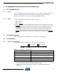
4.3.1 Writing Data to the Device
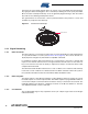
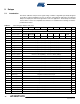
The sequence of events required to write data to the device is shown next.
1. The host initiates the transfer by sending the START condition
2. The host follows this by sending the slave address of the device together with the
WRITE bit.
Table 4-1. Description of Write Data Bits
Key Description
S START condition
SLA+W Slave address plus write bit
A Acknowledge bit
MemAddress Target memory address within device
Data Data to be written
P Stop condition
SLA+W
MemAddress
AAS
Data A P
Host to Device Device to Host