
Datasheet

24
9596A–AT42–10/10
AT42QT1070
6. Specifications
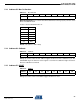
6.1 Absolute Maximum Specifications
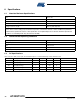
6.2 Recommended Operating Conditions
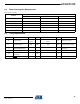
6.3 DC Specifications
Vdd -0.5 to +6V
Max continuous pin current, any control or drive pin ±10 mA
Short circuit duration to ground, any pin infinite
Short circuit duration to Vdd, any pin infinite
Voltage forced onto any pin -0.5V to (Vdd + 0.5) Volts
CAUTION: Stresses beyond those listed under Absolute Maximum Specifications may cause permanent damage to the
device. This is a stress rating only and functional operation of the device at these or other conditions beyond those
indicated in the operational sections of this specification is not implied. Exposure to absolute maximum specification
conditions for extended periods may affect device reliability.
Operating temperature -40
o
C to +85
o
C
Storage temperature -55
o
C to +125
o
C
Vdd +1.8V to 5.5V
Supply ripple+noise ±25 mV
Cx load capacitance per key 1 to 30 pF
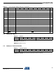
Vdd = 3.3V, Cs = 10nF, load = 5 pF, 32 ms default sleep, Ta = recommended range, unless otherwise noted
Parameter Description Minimum Typical Maximum Units Notes
Vil Low input logic level – – 0.2Vdd V
Vih High input logic level 0.7Vdd – Vdd + 0.5 V
Vol Low output voltage – – 0.6 V
Voh High output voltage Vdd - 0.7V – – V
Iil Input leakage current – – ±1 µA