PL-2303HX Edition (Chip Rev D) USB to Serial Bridge Controller Product Datasheet Document Revision: 1.1 Document Release: April 16, 2007 Prolific Technology Inc. 7F, No. 48, Sec. 3, Nan Kang Rd. Nan Kang, Taipei 115, Taiwan, R.O.C. Telephone: +886-2-2654-6363 Fax: +886-2-2654-6161 E-mail: sales@prolific.com.tw Website: http://www.prolific.com.
Revised Date: April 16, 2007 ds_pl2303HXD_v1.1.doc Disclaimer All the information in this document is subject to change without prior notice. Prolific Technology Inc. does not make any representations or any warranties (implied or otherwise) regarding the accuracy and completeness of this document and shall in no event be liable for any loss of profit or any other commercial damage, including but not limited to special, incidental, consequential, or other damages.
Revised Date: April 16, 2007 ds_pl2303HXD_v1.1.doc Revision History Revision Description Date ¾ Added Windows Vista and XP Logo Driver information April 16, 2007 ¾ Added USB-IF Logo TID information 1.0B ¾ Sec. 4.2: Modified QFN diagram to add IC bottom PAD information June 30, 2006 1.0A ¾ PL-2303HX (Chip Rev D) Datasheet – Formal Release November 23, 2005 1.1 PL-2303HX (Rev D) Product Datasheet -3- Document Version 1.
Revised Date: April 16, 2007 ds_pl2303HXD_v1.1.doc Table of Contents 1.0 FEATURES........................................................................................................8 2.0 FUNCTIONAL BLOCK DIAGRAM....................................................................9 3.0 INTRODUCTION .............................................................................................10 4.0 PIN ASSIGNMENT OUTLINE ......................................................................... 11 4.
Revised Date: April 16, 2007 ds_pl2303HXD_v1.1.doc 11.0 REEL PACKING INFORMATION..................................................................... 25 11.1 Carrier Tape (SSOP-28) ...................................................................................... 25 11.2 Reel Dimension ................................................................................................... 26 12.0 ORDERING INFORMATION ...........................................................................
Revised Date: April 16, 2007 ds_pl2303HXD_v1.1.doc List of Figures Figure 2-1 Block Diagram of PL-2303HX (Rev D).................................................................... 9 Figure 4-1 Pin Assignment Outline of PL-2303HX (Rev D) SSOP28 ......................................11 Figure 4-2 Pin Assignment Outline of PL-2303HX (Rev D) QFN32 ....................................... 12 Figure 10-1 Power-On Reset Diagram ...................................................................................
Revised Date: April 16, 2007 ds_pl2303HXD_v1.1.doc Table 10-1 Package Dimension .............................................................................................. 23 Table 11-2 Reel Part Number Information............................................................................... 26 Table 12-1 Ordering Information ............................................................................................. 26 PL-2303HX (Rev D) Product Datasheet -7- Document Version 1.
Revised Date: April 16, 2007 ds_pl2303HXD_v1.1.doc 1.0 Features ¾ Fully Compliant with USB Specification v2.0 (Full-Speed) ¾ On Chip USB 1.1 transceiver, 5VÆ3.
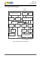
Revised Date: April 16, 2007 ds_pl2303HXD_v1.1.doc 2.0 Functional Block Diagram USB Host USB 1.1 Transceiver 96MHz Clock Generator Power Management Control Endpoint USB Digital Lock Loop USB to Serial Interface Engine Bulk-in Endpoint Bulk-Out Endpoint 256/384Byte Inbound Data Buffer 256/128Byte Outbound Data Buffer Interrupt Endpoint 256-Bytes OTP ROM 5 to 3.
Revised Date: April 16, 2007 ds_pl2303HXD_v1.1.doc 3.0 Introduction PL-2303HX provides a convenient solution for connecting an RS232-like full-duplex asynchronous serial device to any Universal Serial Bus (USB) capable host. PL-2303HX highly compatible drivers could simulate the traditional COM port on most operating systems allowing the existing applications based on COM port to easily migrate and be made USB ready.
Revised Date: April 16, 2007 ds_pl2303HXD_v1.1.doc 4.0 Pin Assignment Outline 4.
Revised Date: April 16, 2007 ds_pl2303HXD_v1.1.doc VD D _325 GN D T EST R ESER VED NC NC T XD D T R _N QFN32 Package R T S_N 4.
Revised Date: April 16, 2007 ds_pl2303HXD_v1.1.doc 5.0 Pin Assignment & Description Pin Type Abbreviation: I: Input 5.
Revised Date: April 16, 2007 ds_pl2303HXD_v1.1.doc 5.
Revised Date: April 16, 2007 ds_pl2303HXD_v1.1.doc 6.0 USB Standard Descriptors PL-2303HX supports one configuration with one interface and four endpoints. The descriptors are basically stored in an internal hardware ROM. However, some fields could be optionally modified by properly programmed on-chip OTPROM. The contents of all descriptors are shown in the following sections and the format of OTPROM would be given in later chapter. 6.
Revised Date: April 16, 2007 ds_pl2303HXD_v1.1.doc Configuration Register 2). If all remote wakeup sources are disabled, the bmAttributes will be 80h. Otherwise, A0h is returned to indicate that this device is Remote Wakeup capable. (4) – The value of maximum power consumption depends on the LD_MODE (bit 5 of Device Configuration Register 2) parameter. If it is set to 1, the MaxPower byte will be FAh for it requires 500mA from the system. Otherwise, it is 32h that indicates 100mA required. 6.
Revised Date: April 16, 2007 ds_pl2303HXD_v1.1.doc 6.6 Endpoint 3 Descriptor: Bulk Data Input endpoint Table 6-6 Endpoint3 Descriptor Offset Field Size Value Description 0 bLength Byte 07h Size of this descriptor (in bytes) 1 bDescriptorType Byte 05h ENDPOINT descriptor type 2 bEndpointAddress Byte 83h Input endpoint 3 bmAttributes Byte 02h Transfer type is BULK 4 wMaxPacketSize Word 0040h 6 bInterval Byte 00h 6.
Revised Date: April 16, 2007 ds_pl2303HXD_v1.1.doc 6.7.3 String Descriptor 2 - Product Table 6-7c String Descriptor – Product Offset Field Size Value Description 0 Blength Byte 30h Size of this descriptor (in bytes) 1 bDescriptorType Byte 03h STRING descriptor type 2 bSTRING ⎯ ⇒ “USB-Serial Controller C” in UNICODE 6.7.
Revised Date: April 16, 2007 ds_pl2303HXD_v1.1.doc 8.0 Data Formats & Programmable Baud Rate Generator The PL-2303HX controller supports versatile data formats and has a programmable baud rate generator. The supported data formats are shown on Table 8-1. The programmable baud rate generator supports baud rates up to 6M bps as shown in Table 8-2. Table 8-1 Supported Data Formats Description Stop bits Parity type Data bits 1 1.
Revised Date: April 16, 2007 ds_pl2303HXD_v1.1.doc 9.0 DC & Temperature Characteristics 9.1 Absolute Maximum Ratings Table 9-1 Absolute Maximum Ratings Items Ratings Power Supply Voltage - VDD_5 -0.3 to 5.5 V Input Voltage of 3.3V I/O -0.3 to VO_33+0.3 V Input Voltage of 3.3V I/O with 5V Tolerance I/O -0.3 to VDD_5+0.3V Output Voltage of 3.3V I/O -0.3 to VDD_5 +0.3 V Storage Temperature -40 to 150 C 9.2 o DC Characteristics 9.2.
Revised Date: April 16, 2007 ds_pl2303HXD_v1.1.doc 9.2.3 Serial I/O Pins Table 9-2c VDD_325@3.3V Serial I/O Pins Parameter Symbol Output Driving Capability Min Typ IDD Power Supply for Serial I/O Pins Max 8 VDD_325 Unit mA 3.0 3.3 3.6 V Input Voltage Low VIL -- -- 0.25* VDD_325 V High VIH 0.7* VDD_325 -- -- V Low VOL -- -- 0.4 V High VOH 2.4 -- -- V Max Unit Output Voltage Table 9-2d VDD_325@2.
Revised Date: April 16, 2007 ds_pl2303HXD_v1.1.doc 9.4 Temperature Characteristics Table 9-4 Temperature Characteristics Parameter Symbol Operating Temperature Min -- Junction Operation Temperature Typ (1) -40 TJ -- -40 25 Max Unit (1) 80 o 105 o C C Note: (1) – Test condition: Baud rate 115200 bps loop testing (4096 bytes/loop, random/fix 0xFF data transfer) over 30 minutes. 9.
Revised Date: April 16, 2007 ds_pl2303HXD_v1.1.doc 10.0 Outline Diagram 10.1 SSOP28 Package Table 10-1 Package Dimension Symbol Millimeter Min Nom Inch Max Min 0.38 0.009 Nom Max b 0.22 0.015 E 7.40 7.80 8.20 0.291 0.307 0.323 E1 5.00 5.30 5.60 0.197 0.209 0.220 L 0.55 0.75 0.95 0.021 0.030 0.037 R1 0.09 D 9.9 0.402 0.413 0.004 10.2 A 10.5 0.390 2.0 0.079 e 0.65 0.0256 L1 1.25 0.050 A1 0.05 A2 1.65 0.020 1.75 1.85 0.065 0.069 0.
Revised Date: April 16, 2007 ds_pl2303HXD_v1.1.doc 10.2 QFN32 Package Figure 10-2 Outline Diagram of PL-2303HX (Rev D) QFN32 PL-2303HX (Rev D) Product Datasheet - 24 - Document Version 1.
Revised Date: April 16, 2007 ds_pl2303HXD_v1.1.doc 11.0 Reel Packing Information 11.1 Carrier Tape (SSOP-28) Figure 11-1a SSOP28 Carrier Tape Notes: 1. 2. 3. 4. 5. 6. 7. 10 sprocket hole pitch cumulative tolerance ±0.2 Camber not to exceed 1mm in 100mm. Material: Black Polystyrene. Ao and Bo measured on a plane 0.3mm above the bottom of the pocket. Ko measured from a plane on the inside bottom of the pocket to the top surface of the carrier.
Revised Date: April 16, 2007 ds_pl2303HXD_v1.1.doc 11.2 Reel Dimension Figure 11-2 Reel Dimension Table 11-2 Reel Part Number Information Part Number Normal Hub Width W1 +0.3mm 16mm 16.8mm RD33008SW-T + RD33008SW-T W2 Max -0.2mm 22.2mm 12.