SUPER SUPER SUPER SUPER SUPER P6DGS P6DGE P6DGU P6SGU USER’S MANUAL Revision 2.
The information in this User’s Manual has been carefully reviewed and is believed to be accurate. The vendor assumes no responsibility for any inaccuracies that may be contained in this document, makes no commitment to update or to keep current the information in this manual, or to notify any person or organization of the updates. Please Note: For the most up-to-date version of this manual, please see our web site at www.supermicro.com.
Preface Preface About This Manual This manual is written for system houses, PC technicians and knowledgeable PC end users. It provides information for the installation and use of the SUPER P6DGS/P6DGE/P6DGU/P6SGU motherboard. The SUPER P6DGS/P6DGE/P6DGU/P6SGU supports Pentium II 233-333 MHz processors at a 66MHz bus speed and Pentium II/III 350-700 MHz processors at a 100MHz bus speed and Slot 1 Celeron processors of up to 466 MHz.
SUPER P6DGS/P6DGE/P6DGU/P6SGU User’s Manual asked questions] section is provided. Instructions are also included for technical support procedure, for returning merchandise for service and for BIOS upgrades. See Chapter 4 for configuration data and BIOS features. Chapter 5 has information on running setup and includes the default settings for Standard Setup, Advanced Setup, Chipset function, Power Management, PCI/PnP Setup and Peripheral Setup.
Preface Table of Contents Preface About This Manual ...................................................................................................... iii Manual Organization ................................................................................................... iii Jumper/Connector Quick Reference ........................................................................ viii Front Control Panel Connector ..................................................................................
SUPER P6DGS/P6DGE/P6DGU/P6SGU User’s Manual Power Supply Connector ........................................................................ 2-7 Secondary Power Connector .................................................................. 2-7 Infrared Connector .................................................................................... 2-7 PW_ON Connector .................................................................................... 2-8 Reset Connector .........................................
Table of Contents Chapter 4: AMIBIOS 4-1 Introduction ....................................................................................................... 4-1 4-2 BIOS Features ................................................................................................. 4-2 BIOS Configuration Summary Screen ................................................... 4-3 AMIBIOS Setup .........................................................................................
SUPER P6DGS/P6DGE/P6DGU/P6SGU User’s Manual Jumper/Connector Quick Reference P6DGS/P6DGE Jumper Function JB1, JB2, JB3, JB4 CPU/Bus Ratio Selection JBT1 CMOS Clear JP20 Power Save State Select JL2 Manufacturer Default JA5 JA1, JA3, SCSI Termination (default on as terminated) JA6 JA2 SCSI Termination (default on as terminated) Bus Speed JP11 P6DGU/P6SGU Page Jumper Function Page 2-6 2-10 2-9 1-3 JB1, JB2, JB3, JB4 JBT1 JP20 S-TERM 2-6 2-10 2-9 1-3 BZ_ON JP11 CPU/Bus Ratio Selection CMOS Clear P
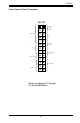
Preface Front Control Panel Connector JF2 JF1 1 1 Hard Drive LED IR Con X Power LED X Keyboard lock Power On X Speaker Reset Please see pages 2-7 through 2-9 for pin definitions.
Preface Notes
Chapter 1: Introduction Chapter 1 Introduction 1-1 Overview The SUPER P6DGS/P6DGE/P6DGU/P6SGU supports Pentium II 233-333 MHz processors at a 66MHz bus speed and Pentium II/III 350-700 MHz processors at a 100MHz bus speed. The SUPER P6DGU/P6DGS/P6DGE supports single or dual Pentium II/III processors and the SUPER P6SGU supports a single Pentium II/III processor.
SUPER P6DGS/P6DGE/P6DGU/P6SGU Manual SUPER P6DGS Figure 1-1.
Chapter 1: Introduction 9.
SUPER P6DGS/P6DGE/P6DGU/P6SGU Manual SUPER P6DGE Figure 1-3.
Chapter 1: Introduction 9.
SUPER P6DGS/P6DGE/P6DGU/P6SGU Manual SUPER P6DGU Figure 1-5.
Chapter 1: Introduction 9.
SUPER P6DGS/P6DGE/P6DGU/P6SGU Manual SUPER P6SGU Figure 1-7.
Chapter 1: Introduction JT1 J1 JT3 1 CPU FAN 1 BZ J32 JA2 1 UW SCSI SCSI Bank1 JA1 1 1 Bank0 Bank2 CPU J19 Parallel Port JA3 JOH1: Overheat LED JT3: Thermal Control Fan JA5,JA6: SCSI Termination Bank3 J21 COM2 Ultra2 LVD/SE ATX POWER J17,J18 USB U2 J20 COM1 1 GX S-TERM 1 FLOPPY IDE 2 IDE 1 1 J22 J16 J15 LINE OUT LINE IN JOH1 BZ_ON 8.
SUPER P6DGS/P6DGE/P6DGU/P6SGU Manual CPU CPU Host Bus AGP Port SDRAM 440GX PCI Slots IO APIC SMBus PIIX4 IDE Ports Power Management SCSI USB Ports ISA Slots SIO BIOS Figure 1-9. 440GX AGP Chipset: System Block Diagram (Dual Processors) Note: This is a general block diagram and may not represent the actual number of slots/CPUs on your motherboard. See the following page for the actual specifications of each board.
Chapter 1: Introduction Features of the P6DGS, P6DGE, P6DGU and P6SGU The following list covers the general features of the SUPER P6DGS, P6DGE, P6DGU and P6SGU. CPU • Single or dual Pentium II 233/266/300/333 MHz processors at 66 MHz bus speed or Pentium II/III 350/400/450/500/550/600/650/700 MHz processors at 100 MHz bus speed (The P6SGU supports only a single Pentium II/ III processor.) Note: Please refer to the support section of our web site for a complete listing of supported processors.
SUPER P6DGS/P6DGE/P6DGU/P6SGU Manual • Hardware BIOS virus protection • Auto-switching voltage regulator for the CPU core • SUPERMICRO SUPER Doctor and (optional) Intel ® LANDesk® Client Manager (LDCM) support ACPI/PC 98 Features • Microsoft OnNow • Slow blinking LED for suspend-state indicator • BIOS support for USB keyboard • Real time clock wake-up alarm • Main switch override mechanism • External modem ring-on Onboard I/O • One 68-pin, 16-bit Ultra2 LVD/SE SCSI connector, one 68-pin,
Chapter 1: Introduction 1-2 Chipset Overview The 440GX chipset, developed by Intel, is the ultimate processor platform targeted for 3D graphics and multimedia applications. Along with System-to-PCI bridge integrated with optimized DRAM controller and data path, the chipset introduces the Accelerated Graphics Port (AGP) interface. AGP is a high performance, component level interconnect targeted at 3D applications and is based on a set of performance enhancements to PCI.
SUPER P6DGS/P6DGE/P6DGU/P6SGU Manual Environmental Temperature Control The thermal control sensor monitors the real-time CPU temperature. It will turn on a back-up fan whenever the CPU temperature exceeds a userdefined threshold. The overheat circuitry runs independently from the CPU. It can continue to monitor for overheat conditions even if the CPU is in sleep mode.
Chapter 1: Introduction Hardware BIOS Virus Protection The system BIOS is protected by hardware so that no virus can infect the BIOS area. The user can only change the BIOS content through the flash utility provided by SUPERMICRO. This feature can prevent viruses from infecting the BIOS area and destroying valuable data. Auto-Switching Voltage Regulator for the CPU Core The switching voltage regulator for the CPU core can support up to 20A of current, with auto-sensing voltage ID ranging from 1.8V to 3.5V.
SUPER P6DGS/P6DGE/P6DGU/P6SGU Manual 1-5 ACPI/PC 98 Features ACPI stands for Advanced Configuration and Power Interface. The ACPI specification defines a flexible and abstract hardware interface that provides a standard way to integrate power management features throughout a PC system, including hardware, operating system and application software. This enables the system to automatically turn on and off peripherals such as CD-ROMs, network cards, hard disk drives and printers.
Chapter 1: Introduction Real Time Clock Wake-Up Alarm The PC may appear to be off when not in use, but it is still capable of responding to preset wake-up events. The user can set a timer in the BIOS to wake-up the system at a predetermined time. Main Switch Override Mechanism When an ATX power supply is used, the power button can function as a system suspend button. When the user presses the power button, the system will enter a SoftOff state.
SUPER P6DGS/P6DGE/P6DGU/P6SGU Manual The SUPER P6DGS/P6DGE/P6DGU/P6SGU accommodates ATX power supplies. Although most power supplies generally meet the specifications required by the CPU, some power supplies are inadequate. It is highly recommended that you use a high quality power supply that meets ATX power supply specification 2.01. Additionally, in areas where noisy power transmission is present, you may choose to install a line filter to separate noise from the computer.
Chapter 1: Introduction 1-8 AIC-7895 MultiChannel TM Single-Chip Ultra SCSI The SUPER P6DGS has an onboard SCSI controller that is 100% compatible with all major operating and hardware platforms. PCI 2.1 and SCAM Level 1 compliance are assured. Two independent SCSI channels provide a per channel data transfer rate of 40 MB/s. Connectors include two 68-pin, 16-bit Ultra Wide SCSI connectors (JA1/JA2) and a 50-pin, 8-bit SCSI connector (JA3).
SUPER P6DGS/P6DGE/P6DGU/P6SGU Manual controller can support external High Voltage Differential (HVD) transceivers only for Ultra data rates. When installing Windows NT, refer to the relevant question/answer in the FAQ section of this manual.
Chapter 2: Installation Chapter 2 Installation 2-1 Static-Sensitive Devices Static-sensitive electric discharge can damage electronic components. To prevent damage to your system board, it is important to handle it very carefully. The following measures are generally sufficient to protect your equipment from static discharge. Precautions • Use a grounded wrist strap designed for static discharge. • Touch a grounded metal object before you remove the board from the anti-static bag.
SUPER P6DGS/P6DGE/P6DGU/P6SGU Manual 2. Install the Universal Retention Mechanism (URM) under the motherboard. Do this before mounting the motherboard into the chassis. Do not screw too tightly. Mount the two black plastic pegs onto the motherboard (Figure 2.1). These pegs will be used to attach the fan heatsink supports. Notice that one hole and the base of one peg are larger than the other hole and peg base. Push each peg into its hole firmly until you hear it "click" into place. Figure 2-1.
Chapter 2: Installation slide into the holes in the heatsink support and that the alignment notch in the SEC cartridge fits over the plug in Slot 1. Push the processor down firmly, with even pressure on both sides of the top, until it is seated. Figure 2-2. Retention Mechanism Top of Processor B C A Do not screw in too tight! 6. Slide the clips on the supports (A) forward until they click into place to hold the pegs securely.
SUPER P6DGS/P6DGE/P6DGU/P6SGU Manual Figure 2-3. Attaching the Fan Power Cable B C A Installation of the Universal Retention Mechanism (URM)* Please Note! Screws and washers attach from the bottom of the board and must be installed before mounting the board to the chassis. (See Figures 2-4 and 2-5.) 1. When installing the URM, make sure that the Left (L) and the Right (R) sides are placed accordingly. 2.
Chapter 2: Installation Figure 2-4. URM and Celeron Installation Supero L R R L Screw holes for retention mechanism URM with arms folded Note: Left and Right arms are defined R Note notch in socket Tab Top view of Celeron cap Figure 2-5.
SUPER P6DGS/P6DGE/P6DGU/P6SGU Manual 2-3 Explanation and Diagram of Jumper/ Connector Connector Pins 3 To modify the operation of the motherboard, jumpers can be used to choose settings. Jumpers create shorts between two pins and change the function of the connector. Pin 1 2 1 Jumper Cap Setting is identified with a square. Pin 1-2 short 2-4 Changing the CPU Speed To change the CPU speed for a Pentium II/III processor, change the jumpers shown on Table 2-1.
Chapter 2: Installation 2-5 Mounting the Motherboard in the Chassis All the motherboards have standard mounting holes to fit different types of chassis. Chassis may come with a variety of mounting fasteners, made of metal or plastic. Although a chassis may have both metal and plastic fasteners, metal fasteners are the most highly recommended because they ground the system board to the chassis. Therefore, use as many metal fasteners as possible for better grounding.
SUPER P6DGS/P6DGE/P6DGU/P6SGU Manual PW_ON Connector The PW_ON connector is located on pins 9 and 10 of JF2. Momentarily contacting both pins will power on/off the system. The user can also configure this button to function as a suspend button. (See BIOS setup information on page 5-13). To turn off the power when set to suspend mode, hold down the power button for at least 4 seconds. See Table 2-5 for pin definitions.
Chapter 2: Installation Table 2-9 Speaker Connector Pin Definitions (JF1) Speaker Connector The speaker connector is located on pins 10 to 13 of JF1. See Table 2-9 for pin definitions. Pin Definition N u m b e r Function + Red wire, Speaker data 10 Key No connection 11 Key 12 Speaker data 13 Power Save State Select Refer to Table 2-10 to set JP20.
SUPER P6DGS/P6DGE/P6DGU/P6SGU Manual ATX Serial Ports Table 2-13 ATX Serial Port Pin Definitions J20 J21 ATX serial port COM1 is located on J20 and serial port COM2 is located on J21. See Table 2-13 for pin definitions. Pin Number Definition Pin Number 1 DCD 6 2 DSR 7 3 Serial In 8 4 RTS 9 5 Serial Out 10 CMOS Clear External Battery Connect an external battery to JBT2. Refer to Table 2-15 for pin definitions. Wake-on-LAN The Wake-on-LAN connector is located on WOL.
Chapter 2: Installation Chassis Intrusion The Chassis Intrusion Detector is located on JL1. See the board layouts and the PC Health Monitoring sections in Chapter One for more information. See Table 2-18 for pin definitions. 2-7 Table 2-18 Chassis Intrusion Detector Pin Definitions (JL1) Pin Number Definition 1 Intrusion Input Ground 2 Open = Default, Closed = Intrusion Installing DIMMs CAUTION Exercise extreme care when installing or removing DIMM modules to prevent any possible damage.
SUPER P6DGS/P6DGE/P6DGU/P6SGU Manual Side View of DIMM Installation into Socket To Install: Insert vertically, press down until it snaps into place. Pay attention to the two notches. PC100 Notches PC100 Notches DIMM Note: Notches should align with the receptive points on the socket DIMM Socket Top View of DIMM Socket To Remove: Use your thumb to gently push the edge of the socket and release the module. Do this on both sides for each module. Figure 2-6.
Chapter 2: Installation two hard disk drives and the SCSI adapter. (Note: most SCSI hard drives are single-ended SCSI devices.) The SCSI ID is determined by jumpers or a switch on the SCSI device. The last internal (and external) SCSI device cabled to the SCSI adapter must be terminated.
SUPER P6DGS/P6DGE/P6DGU/P6SGU Manual Table 2-22 68-pin Single Ended SCSI Connector Pin Definitions SCSI Connectors There are no jumpers to configure the onboard Single Ended SCSI interface. Refer to Table 2-22 for pin definitions. Refer to Table 2-23 for the pin definitions of the 50-pin SCSI interface. (See board layouts for the names and locations of SCSI connectors.
Chapter 2: Installation Table 2-24 68-Pin LVD SCSI Connector Pin Definitions Connector Contact Number Signal Names Connector Contact Number Signal Names 1 2 3 4 5 6 7 8 9 10 11 12 13 14 15 16 17 18 19 20 21 22 23 24 25 26 27 28 29 30 31 32 33 34 +DB(12) +DB(13) +DB(14) +DB(15) +DB(P1) +DB(0) +DB(1) +DB(2) +DB(3) +DB(4) +DB(5) +DB(6) +DB(7) +DB(P) GROUND DIFFSENS TERMPWR TERMPWR RESERVED GROUND +ATN GROUND +BSY +ACK +RST +MSG +SEL +C/D +REQ +I/O +DB(8) +DB(9) +DB(10) +DB(11) 35 36 37 38 39 40 41 42 4
SUPER P6DGS/P6DGE/P6DGU/P6SGU Manual Table 2-25 AGP Port Pin Definitions (J8) Pin # B 1 Spare 2 5.0V 3 5.0V 4 USB+ 5 GND 6 INTB# 7 CLK 8 REQ# 9 VCC3.3 10 ST0 11 ST2 12 RBF# 13 GND 14 Spare 15 SBA0 16 VCC3.3 17 SBA2 18 SB_STB 19 GND 20 SBA4 21 SBA6 22 KEY 23 KEY 24 KEY 25 KEY 26 AD31 27 AD29 28 VCC3.3 29 AD27 30 AD25 31 GND 32 AD_STB1 33 AD23 A Pin # B A 12V 34 Vddq3.3 Vddq3.3 Spare 35 AD21 AD22 Reserved* 3 6 AD19 AD20 USB37 GND GND GND 38 AD17 AD18 INTA# 39 C/BE2# AD16 RST# 40 Vddq3.3 Vddq3.
Chapter 3: Troubleshooting Chapter 3 Troubleshooting 3-1 Troubleshooting Procedures Use the following procedures and chart to troubleshoot your system. If you have followed all of the procedures below and still need assistance, refer to the ‘Technical Support Procedures’ and/or ‘Returning Merchandise for Service’ section(s) in this chapter. Before Power On 1. Make sure no short circuits exist between the motherboard and chassis. 2. Disconnect all ribbon/wire cables from the motherboard. 3.
SUPER P6DGS/P6DGE/P6DGU/P6SGU Manual No Power 1. Make sure the default jumper is on and the CPU is correctly set up. 2. Turn the power switch on and off to test the system. 3. If power is still not on, turn off system power to move jumper setting on JP20 from 2-3 to 1-2. 4. If moving the jumper setting has not helped, clear CMOS. 5. Check the power supply voltage monitor. (Check the power supply 115 V / 230 V switch.) No Video Use the following steps for troubleshooting your system configuration.
Chapter 3: Troubleshooting Losing the System’s Setup Configuration 1. Check the setting of jumper JBT1. Ensure that you are using a high quality power supply. A poor quality power supply may cause the system to lose the CMOS setup information. Refer to Chapter 1 of this manual for details. 2. If the above step does not fix the Setup Configuration problem, contact your vendor for repairs. 3-2 Technical Support Procedures 1.
SUPER P6DGS/P6DGE/P6DGU/P6SGU Manual 3-3 Frequently Asked Questions Question: What are the differences between the various memories that the 440GX motherboard can support? Answer: The 440GX integrates a main memory DRAM controller that supports a 64-bit or 72-bit (64 bits of memory data plus 8 ECC bits.) DRAM from 8 MB to 512 MB for SDRAM and from 8 MB to 2 GB SDRAM/registered DIMMs. DRAM types supported are either Synchronous DRAM (SDRAM) or Registered DIMM modules. Please note the following: 1.
Chapter 3: Troubleshooting Question: After flashing the BIOS my system does not have video. How can I correct this? Answer: If the system does not have video after flashing your new BIOS, it indicates the flashing procedure failed. To remedy this, first clear the CMOS per instructions in this manual and retry BIOS flashing procedure. If you still do not have video, please use the following BIOS recovery procedure.
SUPER P6DGS/P6DGE/P6DGU/P6SGU Manual Question: Why can't I turn off the power using the momentary power on/off switch? Answer: The instant power off function is controlled by the BIOS. When this feature is enabled in the BIOS, the motherboard will have instant off capabilities as long as the BIOS has control of the system.
Chapter 3: Troubleshooting 2. When you are prompted to specify the mass storage devices, press S. 3. Provide the driver disks included with the motherboard. Also refer to article ID# Q192163 in Microsoft's Knowledge Base web site. Question: Do I need to change a jumper or BIOS setting for running dual processors? Answer: No jumper or BIOS setting changes are necessary whether running a single or dual processor on the P6DGS/P6DGE/P6DGU board.
SUPER P6DGS/P6DGE/P6DGU/P6SGU Manual Notes 3-8
Chapter 4: AMIBIOS Chapter 4 AMIBIOS 4-1 Introduction This chapter describes the AMIBIOS for Intel 440GX Pentium II/III 600/550/ 500/450/400/350/333/300/266/233 MHz processors. The AMI ROM BIOS is stored in the Flash EEPROM and is easily upgraded using a floppy diskbased program. System BIOS The BIOS is the Basic Input Output System used in all IBM® PC, XT™, AT ® , and PS/2 ® compatible computers. WinBIOS is a high-quality example of a system BIOS.
BIOS User's Manual American Mega Trends SUPER AMIBIOS (c) 1997 American Megatrends, Inc. y Energ 0404981500 Pentium II Motherboard Made in USA R1.0 Checking NVRAM BIOS date code xxxxx KB OK BIOS revision code Hit if you want to run SETUP (C) Super Micro Computer, Inc., XX-XXXX-XXXXXX-XXXXXXXX-XXXXXX-XXXX-X 4-2 BIOS Features • supports Plug and Play V1.0A and DMI 2.1 • supports Intel PCI 2.
Chapter 4: AMIBIOS • five positive voltage inputs • two negative voltage inputs • three fan speed monitoring inputs BIOS Configuration Summary Screen AMIBIOS displays a screen that looks similar to the following when the POST routines complete successfully. AMIBIOS System Configuration (C) 1985-1997 American Megatrends Inc.
BIOS User's Manual Figure 4-1. Standard Option Highlighted Figure 4-2.
Chapter 5: Running Setup Chapter 5 Running Setup* *Optimal and Fail-Safe default settings are bolded in text unless otherwise noted. The WinBIOS Setup options described in this section are selected by choosing the appropriate high-level icon from the Standard Setup screen. All displayed icons are described in this section, although the screen display is often all you need to understand how to set the options.
BIOS User's Manual not workproperly. If you are absolutely certain that you know the drive's PIO mode, select PIO mode 0-4, as appropriate CD ROM Select Type. Select CDROM . Click on OK when AMIBIOS displays the drive parameters. Entering Drive Parameters You can also enter the hard disk drive parameters. The drive parameters are: Parameter Type Cylinders Heads Description The number for a drive with certain identification parameters. The number of cylinders in the disk drive. The number of heads.
Chapter 5: Running Setup 3½ inch, 1.44 MB 3½ inch or 2.88 MB 3½ inch. Note: The Optimal and Fail-Safe settings for Floppy Drive A are 1.44 MB 3 1/2 inch and for Floppy Drive B are Not Installed . 5-1-2 Advanced Setup Quick Boot The Settings are Disabled or Enabled. Set to Enabled to permit AMIBIOS to boot quickly when the computer is powered on. This option replaces the old Above 1 MB Memory Test Advanced Setup option.
BIOS User's Manual 1st Boot Device 2nd Boot Device 3rd Boot Device The options for 1st Boot Device are Disabled, 1st IDE-HDD, 2nd IDEHDD, 3rd IDE-HDD, 4th IDE-HDD, Floppy, ARMD-FDD, ARMD-HDD, ATAPI CD ROM, SCSI, Network or I 20. The options for 2nd Boot Device are Disabled, 1st IDE-HDD, 2nd IDE-HDD, 3rd IDE-HDD, 4th IDE-HDD, Floppy, ARMD-FDD, ARMD-HDD or ATAPI CD ROM. The options for 3rd Boot Device are Disabled, 1st IDE-HDD, 2nd IDE-HDD, 3rd IDEHDD, 4th IDE-HDD, Floppy, ARMD-FDD, ARMD-HDD or ATAPI CDROM.
Chapter 5: Running Setup Display Mode at Add-on ROM Init This option determines the display mode during add-on ROM (except Video add-on ROM) initialization. The settings for this option are Force BIOS or Keep Current. If selected as Force BIOS, the POST will force the display to be changed to BIOS mode before giving control to any addon ROM. If no add-on ROM is found, then the current display mode will remain unchanged even if this setup question is selected as Force BIOS.
BIOS User's Manual password prompt appears every time the computer is turned on. If Setup is chosen, the password prompt appears if WinBIOS Setup is executed. Boot to OS/2 If DRAM size is over 64 MB, set this option to Yes to permit AMIBIOS to run with IBM OS/2. The settings are No or Yes. CPU Microcode Updation Set this option to Enabled to permit the CPU to be updated on line. The settings for this option are Enabled or Disabled .
Chapter 5: Running Setup C800, 16K Shadow CC00, 16K Shadow D000, 16K Shadow D400, 16K Shadow D800, 16K Shadow DC00, 16K Shadow These options enable shadowing of the contents of the ROM area named in the option. The ROM area not used by ISA adapter cards is allocated to PCI adapter cards. The settings are: Disabled , Enabled or Cached . When set to Disabled, the contents of the video ROM are not copied to RAM.
BIOS User's Manual outside of main DRAM range (i.e. in the 640k - 1M range or above TOM) - The GX can assert SERR# upon detecting an invalid AGP master access outside of AGP aperture. - The GX asserts SERR# for one clock when it detects a target abort during GX initiated AGP cycle PERR# This option signals data parity errors of the PCI bus. The settings are Enabled or Disabled. Set to Enabled to enable the PERR# signal.
Chapter 5: Running Setup Memory Autosizing Support The dynamic detection and sizing of SDRAM and EDO is performed by the BIOS in a system populated with memory which has no SPD information. When set to Enable , memory does not have the SPD information. The settings for this option are Auto or Enable . DRAM Integrity Mode The settings for this option are None , EC or ECC Hardware. Note: For ECC memory only. See the table below to set the type of system memory checking.
BIOS User's Manual DRAM Refresh Rate This option specifies the interval between Refresh signals to DRAM system memory. The settings for this option are 15.6 us (micro-seconds), 31.2 us , 62.4 us , 124.8 us or 249.6 us . Memory Hole This option specifies the location of an area of memory that cannot be addressed on the ISA bus. The settings are Disabled , 15 MB- 16 MB , or 512 KB -640 KB. SDRAM CAS# Latency This option regulates the column address strobe. The settings are 2 SCLKs, 3 SCLKs or Auto .
Chapter 5: Running Setup Gated Clock Signal GCLKEN enables internal dynamic clock gating in the GX when a AGPset "IDLE" state occurs. This happens when the GX detects an idle state on all its buses. The settings for this option are Enabled or Disabled. The Enabled setting enables the gated clock. Graphics Aperture Size This option specifies the amount of system memory that can be used by the Accelerated Graphics Port (AGP). The settings are 4 MB , 8 MB, 16 MB, 32 MB, 64 MB, 128 MB, or 256 MB.
BIOS User's Manual 8bit I/O Recovery Time This option specifies the length of a delay inserted between consecutive 8-bit I/O operations. The settings are Disabled , 1 SYSCLK , 2 SYSCLKs , 3 SYSCLKs, 4 SYSCLKs, 5 SYSCLKs, 6 SYSCLKs, 7 SYSCLKs or 8 SYSCLKs . 16bit I/O Recovery Time This option specifies the length of a delay inserted between consecutive 16-bit I/O operations. The settings are Disabled , 1 SYSCLK, 2 SYSCLKs , 3 SYSCLKs, 4 SYSCLKs, 5 SYSCLKs, 6 SYSCLKs, 7 SYSCLKs or 8 SYSCLKs.
Chapter 5: Running Setup DMA6 Type DMA7 Type These options specify the bus that the specified DMA channel can be used on. The settings are PC/PCI , Distributed, or Normal ISA . Memory Buffer Strength The settings for this option are Strong or Auto . Manufacturer's Setting Note: The user should always set this option to mode 0. modes are for factory testing only . 5-1-4 All other Power Management Power Management The settings for this feature are: APM, ACPI or Disabled.
BIOS User's Manual Hard Disk Power Down Mode This option specifies the power conserving state that the hard disk drive enters after the specified period of hard drive inactivity has expired. The settings are Disabled , Standby , or Suspend . Note: The Optimal default setting for this option is Suspend and the Fail-Safe default setting is Disabled . Hard Disk Timeout (Minutes) This option specifies the length of a period of hard disk drive inactivity.
Chapter 5: Running Setup no display activity for the length of time specified in the Standby Timeout (Minute) option, the computer enters a power savings state. The settings are Monitor or Ignore .
BIOS User's Manual PCI VGA Palette Snoop The settings for this option are Disabled or Enabled. When set to Enabled, multiple VGA devices operating on different buses can handle data from the CPU on each set of palette registers on every video device. Bit 5 of the command register in the PCI device configuration space is the VGA Palette Snoop bit (0 is disabled).
Chapter 5: Running Setup PCI Slot1 IRQ Priority PCI Slot2 IRQ Priority PCI Slot3 IRQ Priority PCI Slot4 IRQ Priority These options specify the IRQ priority for PCI devices installed in the PCI expansion slots. The settings are Auto, (IRQ) 3, 4, 5, 7, 9, 10, or 11, in priority order . DMA Channel 0 DMA Channel 1 DMA Channel 3 DMA Channel 5 DMA Channel 6 DMA Channel 7 These DMA channels control the data transfers between the I/O devices and the system memory.
BIOS User's Manual Reserved Memory Size This option specifies the size of the memory area reserved for legacy ISA adapter cards. The settings are Disabled , 16K , 32K or 64K . Reserved Memory Address This option specifies the beginning address (in hex) of the reserved memory area. The specified ROM memory area is reserved for use by legacy ISA adapter cards. The settings are C0000 , C4000 , C8000 , CC000, D0000 , D4000, D8000 or DC000. Default Primary Video This feature supports multiple displays.
Chapter 5: Running Setup H/W Monitor In0 (CPU 1) H/W Monitor In1 (CPU 2) H/W Monitor In2 (+3.3V) H/W Monitor In3 (+5V) H/W Monitor In4 (+12V) H/W Monitor In5 (-12V) H/W Monitor In6 (-5V) CPU1 Fan CPU2 Fan Thermal Control Fan The above features are for PC Health Monitoring. The motherboards with W83781D have seven on-board voltage monitors for the CPU core, CPU I/ O, +3.3V, +5V, -5V, +12V, and -12V, and three fan status monitors.
BIOS User's Manual Parallel Port Mode This option specifies the parallel port mode. The settings are Normal , BiDir, EPP or ECP. When set to Normal, the normal parallel port mode is used. Use Bi-Dir to support bidirectional transfers. Use EPP (Enhanced Parallel Port) to provide asymmetric bidirectional data transfer driven by the host device. Use ECP (Extended Capabilities Port) to achieve data transfer rates of up to 2.5 Mbps. ECP uses the DMA protocol and provides symmetric bidirectional communication.
Chapter 5: Running Setup The password check option is enabled in the Advanced Setup by choosing either Always or Setup . The password is stored in CMOS RAM. You can enter a password by typing the password on the keyboard, selecting each letter via the mouse, or selecting each letter via the pen stylus. Pen access must be customized for each specific hardware platform. When you select Supervisor or User, AMIBIOS prompts for a password.
BIOS User's Manual 5-4-2 Fail-Safe Default The Fail-Safe default settings consist of the safest set of parameters. Use them if the system is behaving erratically. They should always work but do not provide optimal system performance characteristics.
Appendix A: BIOS Error Beep Codes Appendix A BIOS Error Beep Codes & Messages During the POST (Power-On Self-Test) routines, which are performed each time the system is powered on, errors may occur. Non-fatal errors are those which, in most cases, allow the system to continue the boot-up process. The error messages normally appear on the screen. Fatal errors are those which will not allow the system to continue the bootup procedure.
BIOS Manual Beeps Error message Description 1 Refresh Failure The memory refresh circuitry on the motherboard is faulty. 2 Parity Error A parity error was detected in the base memory (the first 64 KB block) of the system. 3 Base 64 KB Memory Failure A memory failure occurred within the first 64 KB of memory. 4 Timer Not Operational A memory failure was detected in the first 64 KB of memory, or Timer 1 is not functioning. 5 Processor Error The CPU on the system board generated an error.
Appendix A: BIOS Error Beep Codes If it beeps... 1, 2, 3 times then ... reseat the DIMM memory. If the system still beeps, replace the memory. 6 times reseat the keyboard controller chip. If it still beeps, replace the keyboard controller. If it still beeps, try a different keyboard, or replace the keyboard fuse, if the keyboard has one. 8 times there is a memory error on the video adapter. Replace the video adapter, or the RAM on the video adapter. 9 times the BIOS ROM chip is bad.
BIOS Manual Error Message Information 8042 Gate -- A20 Gate A20 on the keyboard controller (8042) Error is not working. Replace the 8042. Address Line Short! Error in the address decoding circuitry on the motherboard. C: Drive Error Hard disk drive C: does not respond. Run the Hard Disk Utility to correct this problem. Also, check the C: hard disk type in Standard Setup to make sure that the hard disk type is correct. C: Drive Failure Hard disk drive C: does not respond.
Appendix A: BIOS Error Beep Codes Error Message Information CMOS Time and Run Standard Setup to set the date and time Date Not Set in CMOS RAM. D: Drive Error Hard disk drive D: does not respond. Run the Hard Disk Utility. Also check the D: hard disk type in Standard Setup to make sure that the hard disk drive type is correct. D: Drive Failure Hard disk drive D: does not respond. Replace the hard disk. Diskette Boot Failure The boot disk in floppy drive A: is corrupt.
BIOS Manual Error Message Information Invalid Boot Diskette The BIOS can read the disk in floppy drive A:, but cannot boot the computer. Use another boot disk. Keyboard Is Locked... The keyboard lock on the computer is Unlock It engaged. The computer must be unlocked to continue. Keyboard Error There is a timing problem with the keyboard. Set the Keyboard options in Standard Setup to Not Installed to skip the keyboard post routines.
Appendix B: AMIBIOS POST Diagnostics Error Messages Appendix B AMIBIOS POST Diagnostic Error Messages This section describes the power-on self-test's (POST) port 80 codes for the AMIBIOS. Check Point Description 00 Code copying to specific areas is done. to INT 19h boot loader next. Passing control 03 NMI is Disabled. power-on condition. 05 The BIOS stack has been built. memory. 06 Uncompressing the post code unit next. 07 Next, initializing the CPU init and the CPU data area.
BIOS Manual Check Point Description 10 The keyboard controller command byte is written. Next, issuing the pin 23 and 24 blocking and unblocking commands. 11 Next, checking if the keys were pressed during power on. Initializing CMOS RAM if the Initialize CMOS RAM in every boot AMIBIOS POST option was set in AMIBCP or the key was pressed. 12 Next, disabling DMA controllers 1 and 2 and interrupt controllers 1 and 2. 13 The video display has been disabled. initialized.
Appendix B: AMIBIOS POST Diagnostics Error Messages Check Point Description 28 Initialization before setting the video mode is complete. Configuring the monochrome mode and color mode settings next. 2A Bus initialization system, static, output devices will be done next, if present. 2B Passing control to the video ROM to perform any required configuration before the video ROM test. 2C All necessary processing before passing control to the video ROM is done.
BIOS Manual Check Point Description 38 Initializing the bus input, IPL, and general devices next, if present. 39 Displaying bus initialization error messages. 3A The new cursor position has been read and saved. Displaying the Hit message next. 40 Preparing the descriptor tables next. 42 The descriptor tables are prepared. mode for the memory test next. 43 Entered protected mode. diagnostics mode next. 44 Interrupts enabled if the diagnostics switch is on.
Appendix B: AMIBIOS POST Diagnostics Error Messages Check Point Description 4C The memory below 1 MB has been cleared via a soft reset. Clearing the memory above 1 MB next. 4D The memory above 1 MB has been cleared via a soft reset. Saving the memory size next. Going to checkpoint 52h next. 4E The memory test started, but not as the result of a soft reset. Displaying the first 64 KB memory size next. 4F The memory size display has started. The display is updated during the memory test.
BIOS Manual Check Point Description 60 The DMA page register test passed. DMA Controller 1 base register test next. 62 The DMA controller 1 base register test passed. Performing the DMA controller 2 base register test next. 65 The DMA controller 2 base register Programming DMA controllers 1 and 2 next. 66 Completed programming DMA controllers 1 and 2. Initializing the 8259 interrupt controller next. 7F Extended NMI source enabling is in progress. 80 The keyboard test has started.
Appendix B: AMIBIOS POST Diagnostics Error Messages Check Point Description 87 The been code Setup programming before WINBIOS Setup has completed. Uncompressing the WINBIOS Setup and executing the AMIBIOS Setup or WINBIOS utility next. 88 Returned from WINBIOS Setup and cleared the screen. Performing any necessary programming after WINBIOS Setup next. 89 The programming after WINBIOS Setup has been completed. Displaying the power-on screen message next.
BIOS Manual Check Point Description 99 Any initialization required after the option ROM test has been completed. Configuring the timer data area and printer base address next. 9A Set the timer and printer base addresses. RS-232 base address next. 9B Returned after setting the RS-232 base address. Performing any required initialization before the Coprocessor test next. 9C Required initialization before the Coprocessor test is over. Initializing the Coprocessor next. 9D Coprocessor initialized.
Appendix B: AMIBIOS POST Diagnostics Error Messages Check Point Description A9 Returned from adaptor ROM at E000h control. Next, performing any initialization required after the E000 option ROM had control. AA Initialization after E000 option ROM control completed. Displaying the system configuration next. AB Building the multiprocessor table, if necessary. POST next. B0 The system configuration is displayed. AC Uncompressing the DMI data and initializing DMI.
BIOS Manual Notes B-10