
Datasheet


General Description
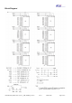
The ADATA’s AD64H1A08 is a 128Mx64 bits 1GB(1024MB) DDR3-1600(CL8) SDRAM over clocking memory
module, The SPD is programmed to JEDEC standard latency 1333Mbps timing of 9-9-9-24 at 1.5V. The module is
composed of eight 128Mx8 bits CMOS DDR3 SDRAMs in FBGA package and one 2Kbit EEPROM in 8pin TDFN
package on a 240pin glass–epoxy printed circuit board.
The AD64H1A08 is a Dual In-line Memory Module and intended for mounting onto 240-pins edge connector
sockets. Synchronous design allows precise cycle control with the use of system clock. Data I/O transactions are
possible on both edges of DQS. Range of operating frequencies, programmable latencies and burst lengths allow
the same device to be useful for a variety of high bandwidth, high performance memory system applications.
Features
• Power supply (Normal): VDD & VDDQ = 1.5V ± 0.075V
• 1.5V (SSTL_15 compatible) I/O
• Timing Reference
- DDR3 1333 CL9-9-9-24 at 1.5V
- DDR3 1600 CL8-8-8-24 at 1.75V
• Burst Length: 4, 8
• Programmable Additive Latency: 0, CL - 2, or CL - 1 clock
• Bi-directional, differential data strobe (DQS and /DQS)
• Differential clock input (CK, /CK) operation
• DLL aligns DQ and DQS transition with CK transition
• Average Refresh Period 7.8us at lower then TCASE 85°C, 3.9us at 85°C < TCASE ≤ 95°C
• 8-bit pre-fetch.
• On Die Termination using ODT pin
•
Internal (self) calibration: Internal self calibration through ZQ pin (RZQ: 240 ohm ± 1%)
• EEPROM VDDSPD=3.3V (Typical)
• PCB Height 30.00mm (1.181”), Single sided component
• Clock Cycle Time (tCK):
- DDR3-1333 tCK=1.5ns
- DDR3-1600 tCK=1.25ns
• Refresh to Active/Refresh Command Time (tRFC): 110ns
• Lead-free products are RoHS compliant
A
D64H1A08
DDR3-1600+(CL8) 240-Pin O.C. U-DIMM
1GB (128M x 64-bits)