
Specifications
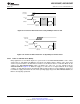
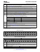


FPGA writes
Control Pins
Power-on
Calibration
On-command
Calibration
Power to
ADC
Calibration
CalDly
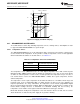
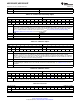
FPGA writes
Control Pins
Power-on
Calibration
On-command
Calibration
Power to
ADC
Calibration
CalDly
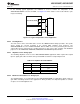
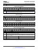
ADC output
valid
ADC12D1000RF, ADC12D1600RF
www.ti.com
SNAS519G –JULY 2011–REVISED APRIL 2013
Figure 6-13. Power-on with Control Pins set by FPGA pre Power-on Cal
Figure 6-14. Power-on with Control Pins set by FPGA post Power-on Cal
6.4.6.2 Power-on and Data Clock (DCLK)
Many applications use the DCLK output for a system clock. For the ADC12D1600/1000RF, each I- and Q-
channel has its own DCLKI and DCLKQ, respectively. The DCLK output is always active, unless that
channel is powered-down or the DCLK Reset feature is used while the device is in Demux Mode. As the
supply to the ADC12D1600/1000RF ramps, the DCLK also comes up, see this example from the
ADC12D1600RFRB: Figure 6-15. While the supply is too low, there is no output at DCLK. As the supply
continues to ramp, DCLK functions intermittently with irregular frequency, but the amplitude continues to
track with the supply. Much below the low end of operating supply range of the ADC12D1600/1000RF, the
DCLK is already fully operational.
Copyright © 2011–2013, Texas Instruments Incorporated Functional Description 61
Submit Documentation Feedback
Product Folder Links: ADC12D1000RF ADC12D1600RF