
Specifications


LM95213
100 pF
ADC12D1600/1000RF
I
R
I
E
= I
F
100 pF
7
6
D1+
D2+
5
D-
FPGA
I
R
I
E
= I
F
ADC12D1000RF, ADC12D1600RF
www.ti.com
SNAS519G –JULY 2011–REVISED APRIL 2013
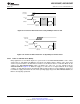
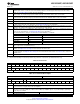
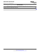
In the following typical application, the LM95213 is used to monitor the temperature of an
ADC12D1600/1000RF as well as an FPGA, see Figure 6-16. If this feature is unused, the Tdiode+/- pins
may be left floating.
Figure 6-16. Typical Temperature Sensor Application
6.4.7.2 Clocking Device
The clock source can be a PLL/VCO device such as the LMX2531LQxxxx family of products. The specific
device should be selected according to the desired ADC sampling clock frequency. The
ADC12D1600RFRB uses the LMX2531LQ1570E, with the ADC clock source provided by the Aux PLL
output. Other devices which may be considered based on clock source, jitter cleaning, and distribution
purposes are the LMK01XXX, LMK02XXX, LMK03XXX and LMK04XXX product families.
6.4.7.3 Amplifiers for the Analog Input
The following amplifiers can be used for ADC12D1600/1000RF applications which require DC coupled
input or signal gain, neither of which can be provided with a transformer coupled input circuit:
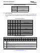
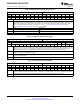
Table 6-12. Amplifier Recommendations
Amplifier Bandwidth Brief features
LMH6552 1.5 GHz Configurable gain
LMH6553 900 MHz Output clamp and configurable
gain
LMH6554 2.8 GHz Configurable gain
LMH6555 1.2 GHz Fixed gain
6.4.7.4 Balun Recommendations for Analog Input
The following baluns are recommended for the ADC12D1600/1000RF for applications which require no
gain. When evaluating a balun for the application of driving an ADC, some important qualities to consider
are phase error and magnitude error.
Copyright © 2011–2013, Texas Instruments Incorporated Functional Description 63
Submit Documentation Feedback
Product Folder Links: ADC12D1000RF ADC12D1600RF