
Specifications
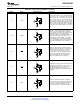


V
A
GND
GND
V
A
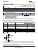
100 k:
ADC12D1800RF
SNAS518I –JULY 2011–REVISED JANUARY 2014
www.ti.com
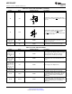
Table 2-2. Control and Status Balls (continued)
Ball No. Name Equivalent Circuit Description
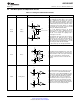
Serial Data-In. In ECM, serial data is shifted into
B4 SDI the device on this pin while SCS signal is asserted
(logic-low).
Serial Data-Out. In ECM, serial data is shifted out
of the device on this pin while SCS signal is
A3 SDO
asserted (logic-low). This output is at TRI-STATE
when SCS is de-asserted.
Do Not Connect. These pins are used for internal
D1, D7, E3, F4,
DNC NONE purposes and should not be connected, i.e. left
W3, U7
floating. Do not ground.
Not Connected. This pin is not bonded and may
C7 NC NONE
be left floating or connected to any potential.
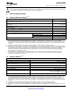
Table 2-3. Power and Ground Balls
Ball No. Name Equivalent Circuit Description
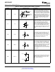
A2, A6, B6, C6,
D8, D9, E1, F1, Power Supply for the Analog circuitry. This supply
H4, N4, R1, T1, V
A
NONE is tied to the ESD ring. Therefore, it must be
U8, U9, W6, Y2, powered up before or with any other supply.
Y6
G1, G3, G4, H2,
J3, K3, L3, M3, Power Supply for the Track-and-Hold and Clock
V
TC
NONE
N2, P1, P3, P4, circuitry.
R3, R4
A11, A15, C18,
D11, D15, D17,
J17, J20, R17,
V
DR
NONE Power Supply for the Output Drivers.
R20, T17, U11,
U15, U16, Y11,
Y15
A8, B9, C8, V8,
V
E
NONE Power Supply for the Digital Encoder.
W9, Y8
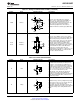
Bias Voltage I-channel. This is an externally
decoupled bias voltage for the I-channel. Each pin
J4, K2 VbiasI NONE should individually be decoupled with a 100 nF
capacitor via a low resistance, low inductance
path to GND.
Bias Voltage Q-channel. This is an externally
decoupled bias voltage for the Q-channel. Each
L2, M4 VbiasQ NONE pin should individually be decoupled with a 100 nF
capacitor via a low resistance, low inductance
path to GND.
16 Device Information Copyright © 2011–2014, Texas Instruments Incorporated
Submit Documentation Feedback
Product Folder Links: ADC12D1800RF