
Specifications
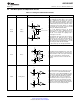


ADC12D1800RF
www.ti.com
SNAS518I –JULY 2011–REVISED JANUARY 2014
These devices have limited built-in ESD protection. The leads should be shorted together or the device placed in conductive foam
during storage or handling to prevent electrostatic damage to the MOS gates.
3 Electrical Specifications
3.1 Absolute Maximum Ratings
(1)(2)
Supply Voltage (V
A
, V
TC
, V
DR
, V
E
) 2.2V
Supply Difference
max(V
A/TC/DR/E
)- min(V
A/TC/DR/E
) 0V to 100 mV
Voltage on Any Input Pin −0.15V to
(except V
IN
+/-) (V
A
+ 0.15V)
V
IN
+/- Voltage Range -0.5V to 2.5V
Ground Difference
max(GND
TC/DR/E
) -min(GND
TC/DR/E
) 0V to 100 mV
Input Current at Any Pin
(3)
±50 mA
ADC12D1800RF Package Power Dissipation at T
A
≤ 65°C
(3)
4.95 W
ESD Susceptibility
(4)
Human Body Model 2500V
Charged Device Model 1000V
Machine Model 250V
Storage Temperature −65°C to +150°C
(1) Absolute Maximum Ratings indicate limits beyond which damage to the device may occur. There is no specification of operation at the
Absolute Maximum Ratings. Operating Ratings indicate conditions for which the device is functional, but do not ensure specific
performance limits. For ensured specifications and test conditions, see the Electrical Characteristics. The ensured specifications apply
only for the test conditions listed. Some performance characteristics may degrade when the device is not operated under the listed test
conditions.
(2) All voltages are measured with respect to GND = GND
TC
= GND
DR
= GND
E
= 0V, unless otherwise specified.
(3) When the input voltage at any pin exceeds the power supply limits, i.e. less than GND or greater than V
A
, the current at that pin should
be limited to 50 mA. In addition, over-voltage at a pin must adhere to the maximum voltage limits. Simultaneous over-voltage at multiple
pins requires adherence to the maximum package power dissipation limits. These dissipation limits are calculated using JEDEC
JESD51-7 thermal model. Higher dissipation may be possible based on specific customer thermal situation and specified package
thermal resistances from junction to case.
(4) Human body model is 100 pF capacitor discharged through a 1.5 kΩ resistor. Machine model is 220 pF discharged through 0Ω.
Charged device model simulates a pin slowly acquiring charge (such as from a device sliding down the feeder in an automated
assembler) then rapidly being discharged.
3.2 Operating Ratings
(1)(2)
Ambient Temperature Range
ADC12D1800RF (Standard JEDEC thermal model) −40°C ≤ T
A
≤ +50°C
ADC12D1800RF (Enhanced thermal model / heatsink) −40°C ≤ T
A
≤ +85°C
Junction Temperature Range - applies only to
maximum operating speed T
J
≤ +120°C
Supply Voltage (V
A
, V
TC
, V
E
) +1.8V to +2.0V
Driver Supply Voltage (V
DR
) +1.8V to V
A
V
IN
+/- Voltage Range
(3)
-0.4V to 2.4V (d.c.-coupled)
V
IN
+/- Differential Voltage Range
(4)
1.0V (d.c.-coupled @100% duty cycle)
2.0V (d.c.-coupled @20% duty cycle)
2.8V (d.c.-coupled @10% duty cycle)
V
IN
+/- Current Range
(3)
±50 mA peak (a.c.-coupled)
(1) Absolute Maximum Ratings indicate limits beyond which damage to the device may occur. There is no specification of operation at the
Absolute Maximum Ratings. Operating Ratings indicate conditions for which the device is functional, but do not ensure specific
performance limits. For ensured specifications and test conditions, see the Electrical Characteristics. The ensured specifications apply
only for the test conditions listed. Some performance characteristics may degrade when the device is not operated under the listed test
conditions.
(2) All voltages are measured with respect to GND = GND
TC
= GND
DR
= GND
E
= 0V, unless otherwise specified.
(3) Proper common mode voltage must be maintained to ensure proper output codes, especially during input overdrive.
(4) This rating is intended for d.c.-coupled applications; the voltages listed may be safely applied to V
IN
+/- for the life-time duty-cycle of the
part.
Copyright © 2011–2014, Texas Instruments Incorporated Electrical Specifications 19
Submit Documentation Feedback
Product Folder Links: ADC12D1800RF