
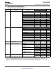
Specifications

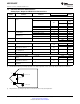
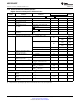


C
IN, DIFF
C
IN, PIN-TO-GND
C
IN, PIN-TO-GND
V
IN
+
V
IN
-
ADC12D1800RF
SNAS518I –JULY 2011–REVISED JANUARY 2014
www.ti.com
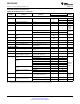
3.6 Converter Electrical Characteristics
Analog Input / Output and Reference Characteristics
ADC12D1800RF
Units
Symbol Parameter Conditions
(Limits)
Typ Lim
Analog Inputs
V
IN_FSR
Analog Differential Input Full Scale Non-Extended Control Mode
Range
FSR Pin High mV
P-P
740
(min)
800
mV
P-P
860
(max)
Extended Control Mode
FM(14:0) = 4000h (default) 800 mV
P-P
FM(14:0) = 7FFFh 1000 mV
P-P
C
IN
Analog Input Capacitance, Differential 0.02 pF
Non-DES Mode
(1)(2)
Each input pin to ground 1.6 pF
Analog Input Capacitance, Differential 0.08 pF
DES Mode
(1)(2)
Each input pin to ground 2.2 pF
R
IN
Differential Input Resistance 91 Ω (min)
100
109 Ω (max)
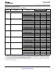
Common Mode Output
V
CMO
Common Mode Output Voltage I
CMO
= ±100 µA 1.15 V (min)
1.25
1.35 V (max)
TC_V
CMO
Common Mode Output Voltage I
CMO
= ±100 µA
(3)
38 ppm/°C
Temperature Coefficient
V
CMO_LVL
V
CMO
input threshold to set See
(3)
0.63 V
DC-coupling Mode
C
L
_V
CMO
Maximum V
CMO
Load Capacitance See
(1)
80 pF
Bandgap Reference
V
BG
Bandgap Reference Output I
BG
= ±100 µA 1.15 V (min)
1.25
Voltage
1.35 V (max)
TC_V
BG
Bandgap Reference Voltage I
BG
= ±100 µA
(3)
32 ppm/°C
Temperature Coefficient
C
L
_V
BG
Maximum Bandgap Reference load See
(1)
80 pF
Capacitance
(1) This parameter is specified by design and is not tested in production.
(2) The differential and pin-to-ground input capacitances are lumped capacitance values from design; they are defined as shown below.
(3) This parameter is specified by design and/or characterization and is not tested in production.
24 Electrical Specifications Copyright © 2011–2014, Texas Instruments Incorporated
Submit Documentation Feedback
Product Folder Links: ADC12D1800RF